HBM– tag –
-

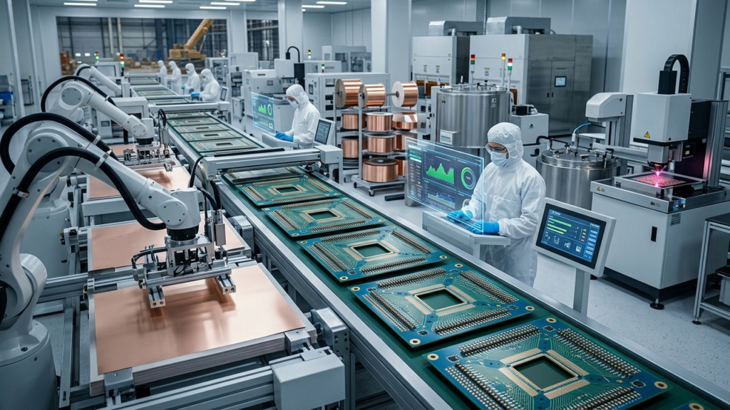
Samsung Electro-Mechanics and Qualcomm Jointly Develop Organic Bridge Technology for 2.1D AI Semiconductor Packaging
The Elec South Korea Overview Samsung Electro-Mechanics and Qualcomm are collaboratively developing an advanced "organic bridge" technology for 2.1D packaging in AI semiconductors. This innovation utilizes organic materials, akin to PCBs... -
Semiconductor Equipment & Materials Market for HBM, Chiplets, and Low-CTE Materials Forecasted to Outpace Overall Wafer Equipment Growth
Mobility Foresights India Overview A Mobility Foresights report projects that the semiconductor equipment and materials market supporting sub-3nm logic, HBM, and chiplet integration will grow faster than the overall wafer equipment marke... -
Panel Warpage Control Emerges as Key Bottleneck Hindering FOPLP Cost Advantage in Advanced Packaging
EAA Partners - Substack USA Overview Panel warpage control is identified as a critical bottleneck preventing Fan-Out Panel Level Packaging (FOPLP) from realizing its theoretical cost advantages in advanced semiconductor manufacturing. Th... -
Advanced AI Chips Face Intensified Thermal Management Challenges: TSMC Plans 20-Layer HBM Integration in 14x Reticle CoWoS by 2028, Microchannel Cooling Emerges as Key Technology
36Kr China Overview Thermal management has become a critical challenge in advanced-packaged AI chips, particularly due to thermal coupling issues across chiplets in 2.5D, 3D IC, CoWoS, and HBM architectures. TSMC's roadmap for 2028 inclu... -
SK Hynix Breakthrough: Mass Reflow Underfill Molding Overcomes HBM Stacking Thermal Challenges, While Micron’s Hybrid Bonding Slashes Power Consumption by 30%
CSIS USA Overview SK Hynix has established a lead in HBM chip stacking by investing heavily in 'Mass Reflow Underfill Molding' (MR-MUF), a novel packaging technique that resolves the thermal and physical constraints of multi-die HBM stac... -
Samsung Electro-Mechanics and Qualcomm Jointly Develop Organic Bridge for Advanced 2.1D AI Semiconductor Packaging
The Elec South Korea Overview Samsung Electro-Mechanics and Qualcomm have collaborated to develop an 'organic bridge' technology for advanced 2.1D packaging in AI semiconductors. This innovation facilitates high-density, high-bandwidth i... -
AI Infrastructure Component Crunch Becomes Reality: ABF Substrate Lead Times Hit 56 Weeks, Equipment Parts Up to 40 Months
BigGo Finance Taiwan Overview The supply shortage for AI infrastructure components is becoming entrenched; TrendForce reports ABF substrate lead times surged to 48–56 weeks, approximately 4 to 4.7 times the equilibrium. HDDs reached 50 w... -
Samsung Electro-Mechanics Unveils Next-Gen Package Substrate Technologies for AI & Servers at KPCA Show 2026, Highlighting Warp Reduction & High-Density Interconnects
Samsung Electro-Mechanics South Korea Overview Samsung Electro-Mechanics showcased a comprehensive suite of next-generation semiconductor package substrate technologies targeting the AI and server markets at 'KPCA Show 2026.' The company... -
AI Accelerator ABF Substrate Shortage to Exceed 40% by 2028; Ibiden, Unimicron, Samsung Electro-Mechanics Rush Billions in Capacity Expansion
Tom's Hardware Japan Overview The supply shortage of ABF (Ajinomoto Build-up Film) substrates for AI accelerators is projected to worsen significantly, potentially reaching approximately 10% by late 2026, 21% by 2027, and over 40% by 202... -
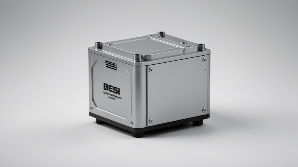
BESI Hybrid Bonding System Orders Exceed 150 Units, HBM5 Onward to Accelerate Memory Adoption
PhotonCap Unknown Overview BESI has secured over 150 cumulative orders for its hybrid bonding systems, with six integrated production lines (including 30 BESI bonders) implemented by major logic customers in partnership with Applied Mate...