
Key Findings
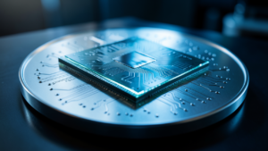
A recent report from Mobility Foresights forecasts that the market for semiconductor equipment and materials supporting next-generation chip manufacturing will expand at a faster rate than the overall wafer manufacturing equipment market. This growth is primarily driven by advancements in sub-3nm logic, high-bandwidth memory (HBM), and chiplet integration technologies, with advanced packaging and bonding techniques, interposers, and specialized HBM packaging materials serving as key growth drivers.
Technical / Clinical Details
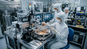
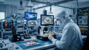
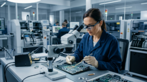
The report details the challenges currently facing semiconductor manufacturing and underscores the critical role of materials and equipment in addressing them. To meet the demands for higher performance and density in chips, advanced packaging and bonding technologies are essential. This includes precise die bonding equipment and interposer technologies for connecting multiple chips. HBM packaging materials are crucial for ensuring thermal management and signal integrity in multi-layer memory stacks. Another significant focus is the development of “Low Coefficient of Thermal Expansion (Low CTE)” materials to mitigate warpage issues in increasingly larger packages. Furthermore, encapsulants for power modules are vital for ensuring reliability in high-power environments, and photonic packaging materials are experiencing rising demand in the emerging field of integrating optical communication with electronic circuits. These advancements in materials and equipment significantly enhance semiconductor device performance and reliability, accelerating the development of applications like AI and HPC.
Background & Context
As the semiconductor industry approaches the limits of Moore’s Law, chip performance improvements are now heavily dependent not just on miniaturization but also on advanced packaging technologies and innovative materials. HBM and chiplet integration exemplify this new paradigm, maximizing overall system performance and efficiency by tightly integrating chips with diverse functionalities. In such complex structures, physical and chemical compatibility among all components is paramount, necessitating material solutions that can overcome challenges related to heat, mechanical stress, and electromagnetic interference.
Strategic Significance & Outlook
This accelerating growth in the semiconductor equipment and materials market is expected to continue. Investment in materials and equipment related to high-performance packaging, in particular, will remain strong. Companies will enhance their competitiveness by focusing on developing low-CTE materials, high-reliability encapsulants, advanced bonding technologies, and photonic packaging solutions. This trend will foster innovation across the entire semiconductor ecosystem, accelerating the realization of next-generation technologies in fields such as AI, autonomous driving, and cloud infrastructure.
Source: https://mobilityforesights.com/blog/making-advanced-chips-euv-etch-deposition
Get our weekly technology intelligence — free
Receive an infographic that lets you judge at a glance whether each field’s analysis report is worth reading.
Subscribe Free — Weekly Tech Intelligence
By subscribing, you’ll receive Troy-Technical’s weekly technology intelligence newsletter.
- Your email and selected fields are used only to deliver the newsletter.
- We never share your information with third parties.
- You can unsubscribe anytime via the link in each email.
See our Privacy Policy for details.
Takes about a minute · Unsubscribe anytime




Comments