Chip– tag –
-

Tyndall National Institute Unveils Three Papers at ESTC 2026 Advancing Photonic Packaging and Chiplet Integration
Tyndall National Institute Ireland Overview Researchers from Tyndall National Institute presented three pivotal papers at ESTC 2026, showcasing significant innovations in photonic packaging, co-packaged optics, and chiplet integration te... -
Taiyo Holdings Achieves First 700nm CD Three-Layer RDL Formation on 12-Inch Wafers with New FPIM Series for Advanced Semiconductor Packaging
Morningstar (Taiyo Holdings Co. Ltd.) Japan Overview Taiyo Holdings has launched its "FPIM Series" next-generation semiconductor-packaging material, achieving the industry's first three-layer Redistribution Layer (RDL) formation with a 7... -
Tata Electronics Invests $3 Billion in India’s First Semiconductor Packaging Facility, Partners with Besi to Boost Advanced Packaging
Tata Electronics India Overview Tata Electronics announced a $3 billion investment in India's first indigenous semiconductor packaging facility in Jagiroad, Assam, and a strategic partnership with advanced packaging equipment provider Be... -
NovoLINC Unveils MaxLINC, Achieving Industry-Leading 0.7 mm²•K/W Thermal Resistance for Multi-Kilowatt AI Chips
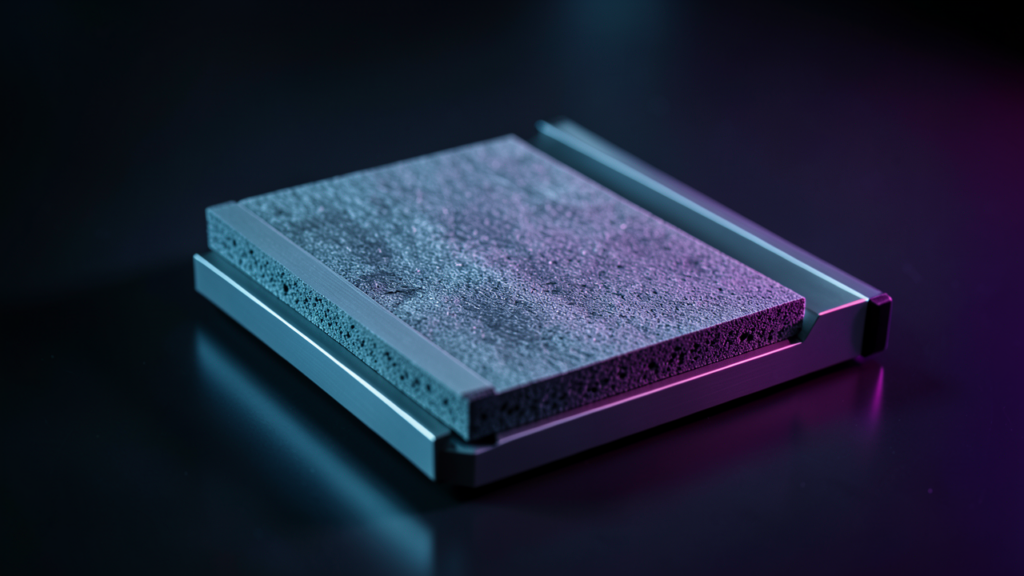
PR Newswire (NovoLINC) Unknown Overview NovoLINC has launched MaxLINC, an advanced thermal interface material (TIM) designed for high-performance AI computing, achieving an industry-leading thermal resistance as low as 0.7 mm²•K/W. This ... -
Samsung Electro-Mechanics and Qualcomm Jointly Develop Organic Bridge Technology for 2.1D AI Semiconductor Packaging
The Elec South Korea Overview Samsung Electro-Mechanics and Qualcomm are collaboratively developing an advanced "organic bridge" technology for 2.1D packaging in AI semiconductors. This innovation utilizes organic materials, akin to PCBs... -
Taiyo Holdings Launches Next-Gen Semiconductor Packaging Material ‘FPIM Series,’ First to Achieve 700nm CD Three-Layer RDL on 12-inch Wafers
PR Newswire Japan Overview Taiyo Holdings, in collaboration with imec, has launched its "FPIM Series," a next-generation semiconductor packaging material that enables the first successful formation of a three-layer Redistribution Layer (... -
Semiconductor Equipment & Materials Market for HBM, Chiplets, and Low-CTE Materials Forecasted to Outpace Overall Wafer Equipment Growth
Mobility Foresights India Overview A Mobility Foresights report projects that the semiconductor equipment and materials market supporting sub-3nm logic, HBM, and chiplet integration will grow faster than the overall wafer equipment marke... -
Advanced AI Chips Face Intensified Thermal Management Challenges: TSMC Plans 20-Layer HBM Integration in 14x Reticle CoWoS by 2028, Microchannel Cooling Emerges as Key Technology
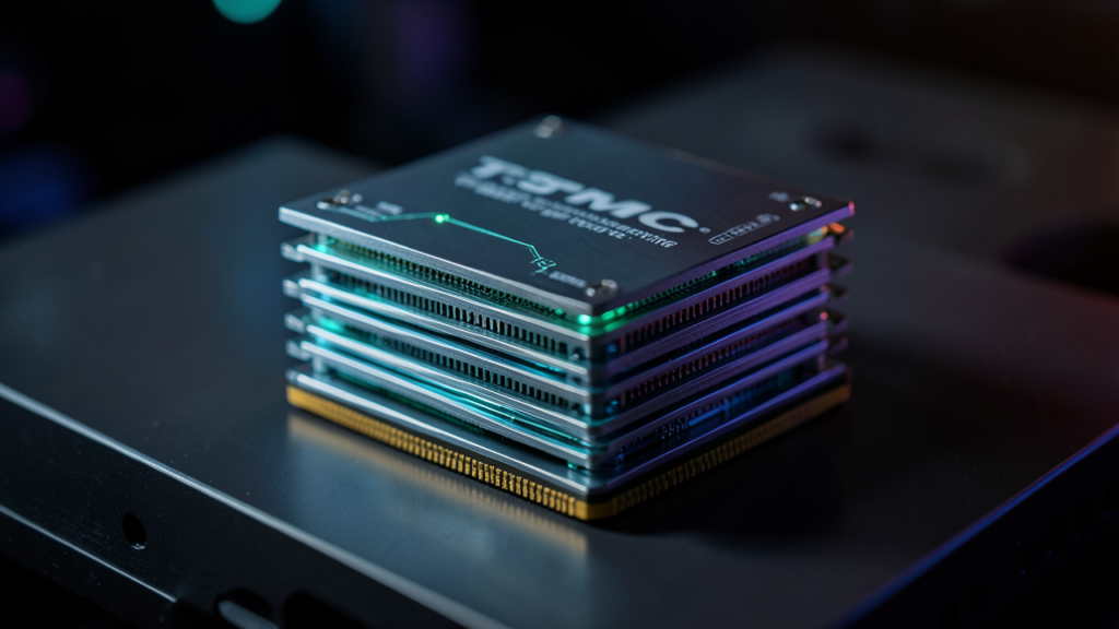
36Kr China Overview Thermal management has become a critical challenge in advanced-packaged AI chips, particularly due to thermal coupling issues across chiplets in 2.5D, 3D IC, CoWoS, and HBM architectures. TSMC's roadmap for 2028 inclu... -
Advanced Packaging Warpage Mitigation: Research Advances in Incorporating Negative Coefficient of Thermal Expansion Materials into Epoxy Molding Compounds and Underfills
Semiconductor Engineering USA Overview Active research is progressing on utilizing negative coefficient of thermal expansion (CTE) materials in epoxy molding compounds (EMC) and underfills to effectively mitigate warpage in large semicon... -
NIST and UCSD Develop Predictive Modeling for Cure Behavior and Thermal Endurance of Advanced Packaging Epoxy Underfills
Semiconductor Engineering USA Overview Researchers from the National Institute of Standards and Technology (NIST) and the University of California San Diego (UCSD) have published a technical paper detailing a new modeling technique to ac...