
Key Findings
Tata Electronics has announced a significant investment of $3 billion to establish India’s first indigenous semiconductor packaging facility in Jagiroad, Assam. Concurrently, the company has formed a strategic partnership with Besi (BE Semiconductor Industries N.V.), a leading provider of advanced packaging equipment and technologies. This dual initiative aims to substantially bolster India’s advanced packaging capabilities within its rapidly developing semiconductor ecosystem.
Technical / Clinical Details
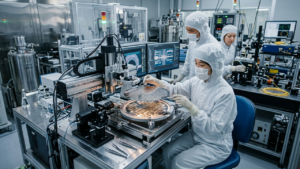
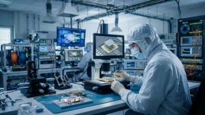
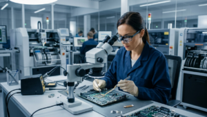
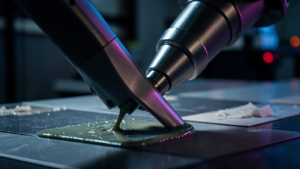
The core of this partnership involves integrating Besi’s state-of-the-art advanced packaging equipment and processes, including die bonding, flip-chip, and surface-mount technologies (SMT), into Tata Electronics’ new facility. Besi’s technologies are renowned for enabling high-precision and high-yield semiconductor device production, from wafer processing to final packaging. This collaboration will specifically accelerate the development of fine-pitch interconnects and advanced thermal management solutions, which are crucial for high-density integrated chips used in AI and high-performance computing (HPC) applications. By doing so, India will establish the capability to manufacture and package complex semiconductor devices domestically, enhancing its position in the global supply chain.
Background & Context
Semiconductors form the backbone of the modern economy, with their importance growing exponentially across sectors like AI, 5G, and IoT. The Indian government, as part of its “Make in India” initiative, has prioritized establishing domestic semiconductor manufacturing capabilities as a national strategic imperative. Currently, India heavily relies on imported semiconductors, which poses geopolitical risks and supply chain vulnerabilities. The partnership between Tata Electronics and Besi is a pivotal step towards overcoming this dependency and building a self-reliant semiconductor ecosystem within India. Besi’s extensive experience globally, including a strong presence in the Asia-Pacific region, makes it an ideal partner for this technological leap.
Strategic Significance & Outlook
This $3 billion investment and strategic alliance with Besi represent a landmark development for India’s semiconductor industry. The new facility is expected to create hundreds of thousands of jobs, fostering further investment in related supply chain companies and research institutions. In the long term, it aims to establish India as a key hub for advanced packaging technology, significantly strengthening the country’s role in the global semiconductor supply chain. This move is essential for India to maintain competitiveness in the future digital economy and enhance its geopolitical autonomy, reducing reliance on external semiconductor manufacturing capabilities.
Get our weekly technology intelligence — free
Receive an infographic that lets you judge at a glance whether each field’s analysis report is worth reading.
Subscribe Free — Weekly Tech Intelligence
By subscribing, you’ll receive Troy-Technical’s weekly technology intelligence newsletter.
- Your email and selected fields are used only to deliver the newsletter.
- We never share your information with third parties.
- You can unsubscribe anytime via the link in each email.
See our Privacy Policy for details.
Takes about a minute · Unsubscribe anytime




Comments