HBM– tag –
-

Taiyo Holdings and imec Unveil 700nm 3-Layer RDL Breakthrough for Next-Gen AI Packaging
Quantum Zeitgeist Japan, Belgium Overview Taiyo Holdings, in collaboration with imec, announced at IEEE ESTC 2026 the successful formation of a 3-layer Redistribution Layer (RDL) with a critical dimension of 700 nanometers on 12-inch waf... -
South Korea Accelerates Advanced Packaging Investments, Establishing Itself as Core of Global AI Semiconductor Supply Chain
Investment Monitor South Korea, USA Overview South Korea is significantly boosting its advanced packaging investments to meet surging AI semiconductor export demand. SK Hynix plans to complete a ₩19 trillion ($12.9 billion) advanced pack... -
Applied Materials Forecasts Over 70% Growth in Advanced Packaging Revenue, Total Revenue Up 40%, Driven by AI and HBM Demand
TradingKey USA Overview Applied Materials projects approximately 40% growth in its total revenue for 2026, benefiting significantly from the increasing complexity in AI chip and HBM manufacturing. The company anticipates over 70% growth ... -
Onto Innovation’s Advanced Packaging Business Achieves 80% Growth, Driven by Dragonfly G5 for HBM4 and 2.5D AI
Investing.com USA Overview Onto Innovation announced its advanced packaging business grew by 80% year-over-year in 2026, fueled by robust demand from HBM and 2.5D logic applications. The company's Dragonfly G5 platform has been adopted f... -
High-End ABF Substrate Supply Faces Critical Shortage Amid Gigantic AI Chip Growth, Fueling Intense Competition Among Taiwanese Manufacturers
Tom's Hardware Taiwan Overview The escalating computational power and physical size of AI chips have led to a severe global shortage in the supply of high-end Ajinomoto Build-up Film (ABF) substrates, a core component. In response, inten... -
TRUMPF Resolves Glass Substrate TGV Coating Bottleneck with High-Power HiPIMS, Accelerating Next-Gen AI Chip Packaging Mass Production
Asianews.network Germany Overview Germany's TRUMPF announced a breakthrough in Through Glass Via (TGV) coating for glass substrates, a critical bottleneck, by leveraging its high-power HiPIMS (High Power Impulse Magnetron Sputtering) tec... -
Samsung Dedicates Half of Its 4nm Foundry Capacity to HBM4 Base Dies Amid AI Boom
ZDNet Korea South Korea Overview Samsung Electronics is reportedly allocating over 50% of its advanced 4nm foundry capacity—specifically 15,000 wafers per month out of an estimated 30,000 total—to the production of HBM4 base dies. This s... -
Hybrid Bonding Equipment Market Projected to Reach $1.73 Billion in 2026, Growing to $2.58 Billion by 2032
360iResearch Global Overview This article provides an overview of a market research report published by 360iResearch. The hybrid bonding equipment market is projected to reach $1.73 billion in 2026, with a compound annual growth rate (CA... -
Micron Reportedly Targets Doubling HBM Capacity to 100,000 Wafers/Month by End-2026, Boosting 12-High HBM4 for NVIDIA Vera Rubin
digitimes USA Overview Micron is reportedly targeting a near-doubling of its High Bandwidth Memory (HBM) production capacity to approximately 100,000 wafers per month by the end of 2026. This significant expansion focuses on ramping up p... -
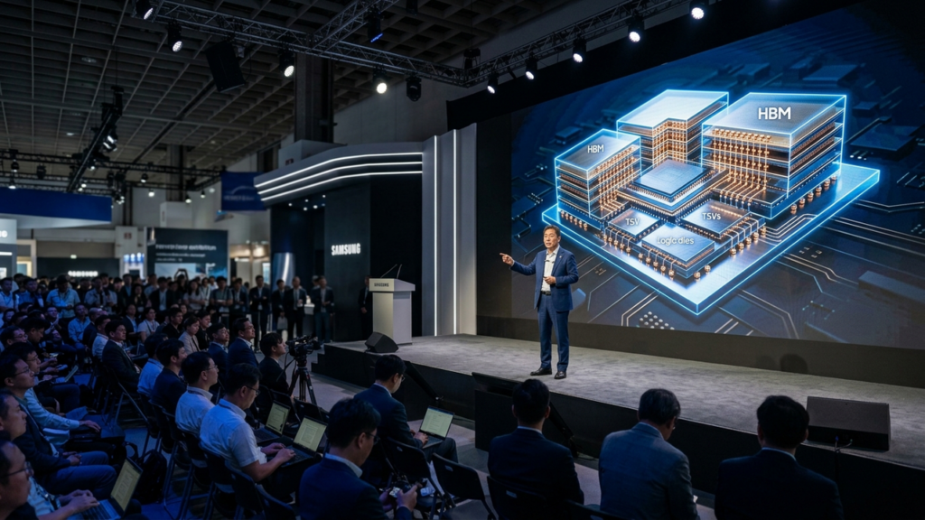
Samsung Unveils 3D-Stacked Memory Strategy, Featuring HBM5, zHBM, and zNAND-O, to Break AI’s Memory Wall
Design And Reuse South Korea Overview At SEMICON Taiwan 2026, Samsung Electronics presented a bold 3D-stacked memory strategy designed to overcome the limitations of current memory architectures in the AI era. This roadmap introduces HBM...