Background: Meeting Escalating Demands in AI and HPC
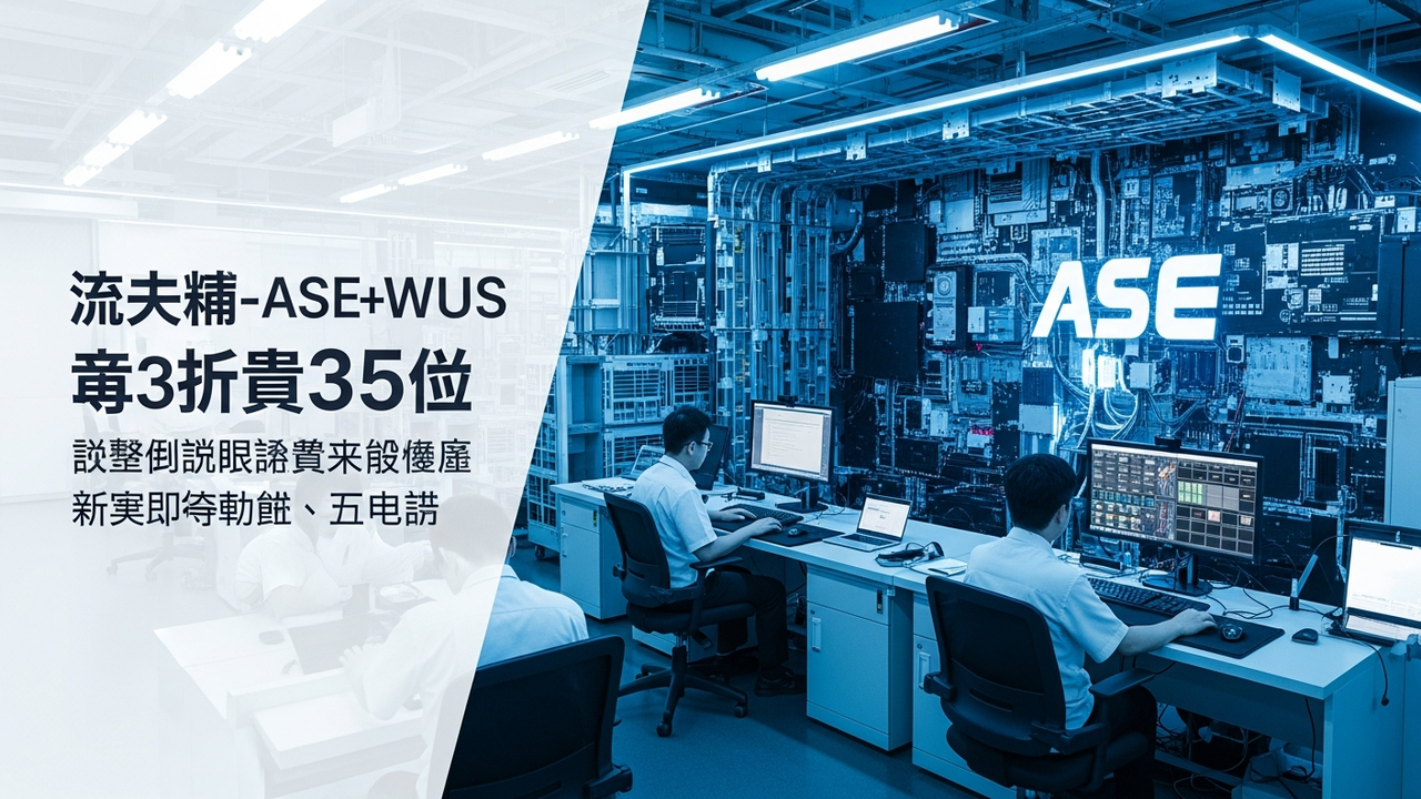
The relentless advancement of Artificial Intelligence (AI), cloud computing, and autonomous driving technologies has placed unprecedented demands on semiconductor packaging innovations. High-performance chips utilized in these applications necessitate sophisticated heterogeneous integration and ultra-high-density interconnect solutions to deliver the required processing power and efficiency. Recognizing this critical market need, ASE Technology Holding, the world’s largest independent outsourced semiconductor assembly and test (OSAT) provider, has partnered with WUS Printed Circuit, a leading printed circuit board (PCB) manufacturer, to establish a new manufacturing hub in Kaohsiung, a pivotal semiconductor industry cluster in Taiwan. This joint venture represents a significant strategic investment, totaling approximately NT$35 billion (around US$1.1 billion).
Overview of the Advanced AI Packaging Hub
The new manufacturing facility, to be located in the Nanzih Technology Industrial Park in Kaohsiung, will specialize in cutting-edge packaging processes essential for next-generation AI chips. Key technologies to be deployed include FOCoS (Fan-out Chip on Substrate) and FC BGA (Flip Chip Ball Grid Array). FOCoS is a type of fan-out packaging technology known for its high-density routing and superior thermal performance, playing a crucial role in chiplet integration and High Bandwidth Memory (HBM) interfaces. FC BGA is a high-density interconnect packaging solution widely adopted for high-performance CPUs, GPUs, and AI accelerators.
The facility is slated for completion by September 2029 and is expected to generate over 2,000 new jobs upon commencing operations. Beyond mere capacity expansion, the project is designed to integrate advanced automated manufacturing processes and smart manufacturing technologies, aiming to optimize productivity, quality, and overall efficiency. This initiative underscores ASE and WUS’s commitment to solidify their leadership positions in the global advanced packaging market.
Industry Impact and Future Outlook
The establishment of this advanced AI packaging hub in Kaohsiung will have substantial implications for Taiwan’s semiconductor industry and the global supply chain. Taiwan, already a global powerhouse in semiconductor manufacturing, will further strengthen its dominance, particularly in the advanced packaging segment crucial for AI. The synergy between ASE’s extensive packaging expertise and WUS’s advanced substrate technology is expected to create a powerful force for overcoming performance bottlenecks in AI chips and accelerating the development of future AI hardware. This hub is poised to become a vital infrastructure component supporting the evolution of AI technologies and contributing to the further advancement of a data-driven society.
Source: https://ase.aseglobal.com/press-room/ase-and-wus-announce-strategic-expansion/







Comments