Key Findings
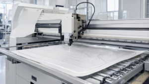
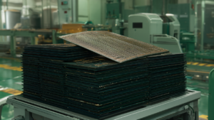
ACM Research has announced that it has received production and evaluation orders from two advanced packaging customers for its self-developed Ultra ECP ap-p horizontal panel-level electroplating tool. This technology is characterized by its unique horizontal electroplating process, which significantly improves uniformity and process stability for various plating processes, including copper, nickel, tin-silver, and gold, on large panel formats up to 600 × 600 mm. This achievement represents a crucial step towards the high-volume manufacturing adoption of large-panel horizontal electroplating in advanced packaging.
Technical / Clinical Details
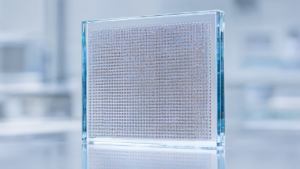
- Large Panel Compatibility: The Ultra ECP ap-p tool supports large panel formats up to 600 × 600 mm. This capability allows for the processing of a significantly greater number of chips simultaneously compared to traditional wafer-level processes, leading to substantial improvements in production efficiency and cost-effectiveness, particularly beneficial for the manufacturing of large packages and System-in-Package (SiP) modules.
- Horizontal Electroplating Technology: The proprietary horizontal electroplating technology ensures highly uniform film thickness and excellent material distribution across the entire panel surface. This leads to reduced defect rates and higher production yields. Furthermore, it mitigates issues such as liquid stagnation and bubble formation, which have been challenges in conventional vertical plating equipment, thereby enhancing process stability.
- Versatile Plating Processes: The tool is compatible with key plating materials widely used in advanced packaging, including copper (Cu), nickel (Ni), tin-silver (SnAg), and gold (Au). This versatility offers customers flexibility in selecting processes to meet diverse application requirements.
Background & Context
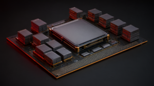
Driven by advancements in AI, High-Performance Computing (HPC), 5G communication, and autonomous driving, semiconductor devices are trending towards higher integration, increased functionality, and larger form factors. To address these demands, packaging technologies are evolving from wafer-level to panel-level processing, necessitating reductions in production costs and increases in capacity. ACM Research’s Ultra ECP ap-p tool is designed to meet this trend, with its performance particularly anticipated for high-density Redistribution Layers (RDLs) and bump formation in advanced packaging.
Strategic Significance & Outlook
Securing production and evaluation orders for the Ultra ECP ap-p horizontal panel electroplating tool marks a significant milestone for ACM Research in establishing its position as a leading equipment provider in the advanced packaging market. The widespread adoption of this technology is expected to enhance the efficiency and quality of panel-level packaging, contributing to the accelerated mass production of next-generation semiconductor devices. This will, in turn, further facilitate the market introduction of high-performance devices, such as AI chips and HPC semiconductors, globally.
Get our weekly technology intelligence — free
Receive an infographic that lets you judge at a glance whether each field’s analysis report is worth reading.
Subscribe Free — Weekly Tech Intelligence
By subscribing, you’ll receive Troy-Technical’s weekly technology intelligence newsletter.
- Your email and selected fields are used only to deliver the newsletter.
- We never share your information with third parties.
- You can unsubscribe anytime via the link in each email.
See our Privacy Policy for details.
Takes about a minute · Unsubscribe anytime