Background
The rapid evolution of artificial intelligence is instigating a profound structural transformation within the semiconductor industry, where the demand for high-bandwidth memory (HBM) consistently outstrips existing supply. SK Hynix, recognized as a pioneer in HBM technology, has solidified its position as a critical supplier to leading AI chip manufacturers, including NVIDIA, thereby securing a dominant market share. While SK Hynix leads, formidable competitors such as Samsung and Micron are also vigorously pursuing HBM4 development and expanding their production capacities, intensifying the competitive landscape within the HBM market. SK Hynix’s substantial investment in the U.S. aligns strategically with U.S. government initiatives promoting domestic semiconductor manufacturing, such as the CHIPS Act, aiming for geographical diversification of the supply chain and contributions to regional economic development.
Key Findings
SK Hynix, capitalizing on its commanding market share exceeding 60% in the High Bandwidth Memory (HBM) sector, has announced an anticipated price increase of approximately 70% for its forthcoming HBM4 generation, slated for 2026. This assertive pricing strategy underscores the exponential surge in AI demand and the prevailing tight supply of HBM. To meet the escalating need for AI memory, the company intends to double its wafer production capacity, which includes establishing a new manufacturing facility in Korea, alongside a significant $3.87 billion (approximately 550 billion KRW) investment in an advanced packaging plant in Indiana, USA. These substantial capital injections, totaling roughly $7 billion, are strategically designed to alleviate existing AI memory supply bottlenecks and accelerate the market introduction of HBM4.
Technical Details: HBM4 Architecture and Performance
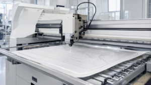
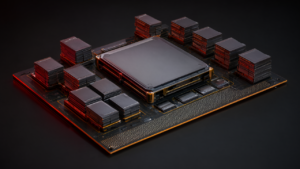
HBM4 is engineered to deliver a substantial uplift in data bandwidth and efficiency over its predecessor, HBM3E. A pivotal feature of HBM4 is its 2048-bit interface width, which is projected to theoretically double the data transfer rate compared to HBM3E’s 1024-bit interface. This expanded interface is crucial for optimizing data flow between AI processors and memory, thereby significantly mitigating computational bottlenecks prevalent in High-Performance Computing (HPC) applications. These applications include, but are not limited to, large language model (LLM) training, high-resolution image processing, and complex scientific simulations. SK Hynix’s advanced packaging facilities will play a critical role in enhancing the miniaturization and reliability of HBM stacking technology, particularly through refined die-to-die connections utilizing Through Silicon Via (TSV) technology. The new Indiana plant is anticipated to not only significantly boost HBM4 production capacity but also forge a resilient supply chain foundation within the U.S., strategically addressing potential geopolitical supply risks. Furthermore, the plan to double wafer production capacity is an essential measure to secure the foundational DRAM chip supply required for HBM and establish a robust mass production system for HBM4.
Strategic Significance and Market Outlook
SK Hynix’s dual strategy of aggressive HBM4 pricing and substantial global investments is set to profoundly reshape the dynamics of the AI memory market. The HBM4’s 2048-bit interface is anticipated to deliver a dramatic performance uplift for AI and HPC applications, thereby enabling the conceptualization and deployment of vastly more complex and data-intensive AI models. The establishment of an advanced packaging facility in the U.S. will serve to fortify the global semiconductor supply chain and ensure a more stable supply of critical AI chips. Industry observers will closely scrutinize how SK Hynix capitalizes on its technological leadership in the HBM4 market to distinguish itself from its rivals. This strategic maneuver is also expected to catalyze new business opportunities for semiconductor equipment manufacturers and material suppliers, further accelerating the overall development of the semiconductor industry in the ongoing AI era.
Source: https://www.facebook.com/fb-answers/sk-hynix-hbm-ai-memory-outlook-2026/
Get our weekly technology intelligence — free
Receive an infographic that lets you judge at a glance whether each field’s analysis report is worth reading.
Subscribe Free — Weekly Tech Intelligence
By subscribing, you’ll receive Troy-Technical’s weekly technology intelligence newsletter.
- Your email and selected fields are used only to deliver the newsletter.
- We never share your information with third parties.
- You can unsubscribe anytime via the link in each email.
See our Privacy Policy for details.
Takes about a minute · Unsubscribe anytime