Background
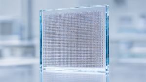
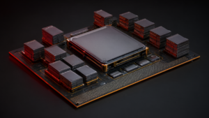
The relentless demand for superior performance in AI chips mandates continuous innovation in advanced packaging, specifically to enhance data transfer speeds and power efficiency between processors and memory. Glass substrates are emerging as a pivotal solution, offering low dielectric loss, exceptional thermal stability, and superior dimensional stability, which are expected to substantially improve data transmission integrity and overall package reliability. This technology holds particular significance for AI accelerators, where the increasing integration of High Bandwidth Memory (HBM) and logic chips positions glass as a potential de facto standard for next-generation designs.
Key Developments
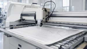
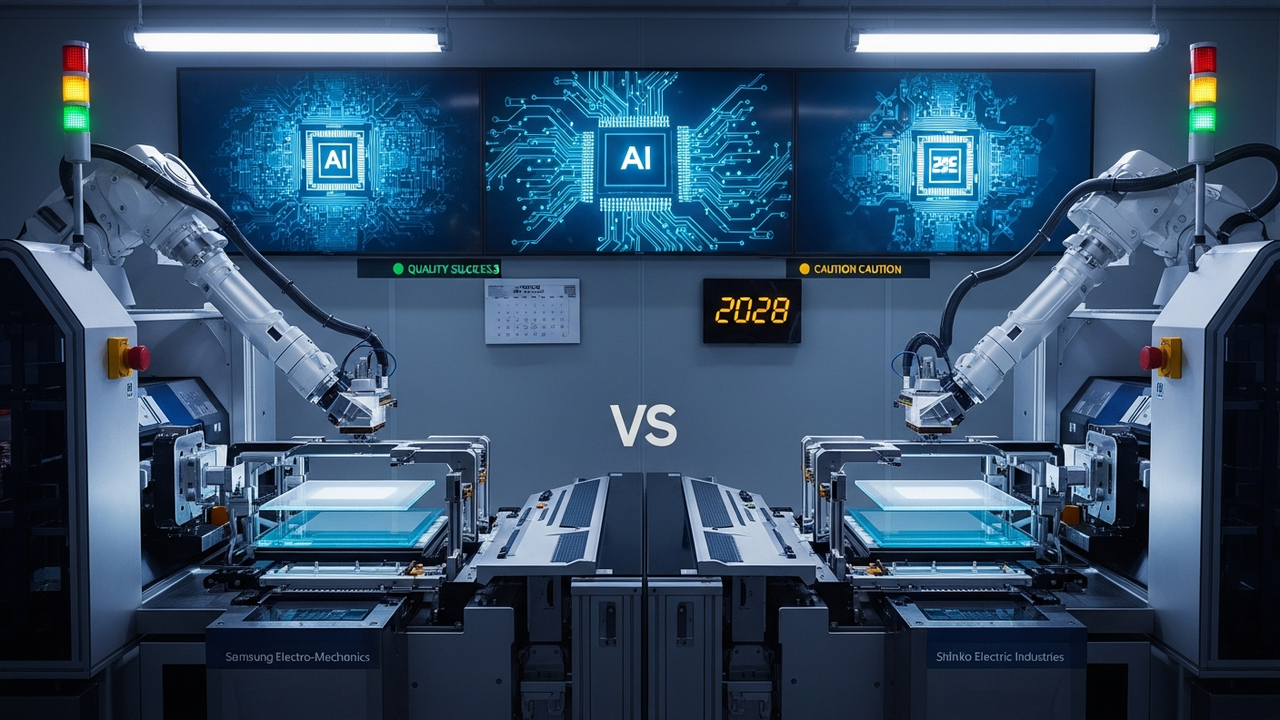
Samsung Electro-Mechanics (SEM) is making aggressive strides towards the mass production of glass substrates for AI chip packaging, setting an ambitious target of 2028. This pursuit, however, is fraught with significant technical challenges, particularly in securing stringent customer quality certifications and achieving consistently stable production yields. To accelerate its efforts, SEM has formed ‘GlaSSEM,’ a joint venture with Dongwoo Fine-Chem, intensifying its direct competition with established Japanese players like Shinko Electric Industries within this critical and burgeoning advanced packaging segment.
Technical Analysis
- Glass substrates present a compelling alternative to conventional organic substrates, primarily by effectively mitigating warpage issues that become pronounced with increasing package area in high-performance AI chips. This intrinsic advantage is critical for enabling higher chip stacking densities and facilitating more complex 3D packaging architectures, thereby cementing glass’s role as a pivotal technology for future AI semiconductors.
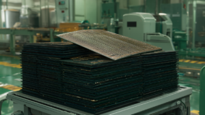
- Samsung Electro-Mechanics is committing substantial research and development resources to cultivate robust glass substrate technology, encompassing advancements from fundamental material science to sophisticated manufacturing processes. The technical challenges are considerable, notably in the fabrication of ultra-fine micro-vias and high-density metal lines on inherently brittle glass, requiring extraordinary precision and the deployment of novel techniques.
- Immediate priorities include securing rigorous quality certifications from tier-one customers and establishing a consistently high yield rate essential for scaling up to mass production. Successfully navigating these formidable technical barriers is imperative for SEM to achieve its ambitious 2028 mass production goal.
Strategic Outlook
The adoption of glass substrate technology is poised to be a determining factor in defining the performance benchmarks of future AI semiconductors. Should Samsung Electro-Mechanics successfully surmount these complex technical hurdles and commence mass production by 2028, it stands to significantly enhance its competitive posture within the advanced packaging market. Nevertheless, given the rapid advancements by rival companies, securing clear superiority in substrate quality, achieving cost-effectiveness, and ensuring robust supply chain stability will be paramount for sustained long-term success in this rapidly burgeoning and highly strategic sector.
Source: #
Get our weekly technology intelligence — free
Receive an infographic that lets you judge at a glance whether each field’s analysis report is worth reading.
Subscribe Free — Weekly Tech Intelligence
By subscribing, you’ll receive Troy-Technical’s weekly technology intelligence newsletter.
- Your email and selected fields are used only to deliver the newsletter.
- We never share your information with third parties.
- You can unsubscribe anytime via the link in each email.
See our Privacy Policy for details.
Takes about a minute · Unsubscribe anytime