Background
Carbon Nanotube (CNT) films are widely recognized as promising components for various advanced electronic and nanostructured materials, including transparent conductive films, flexible electronics, sensors, and energy storage devices, owing to their exceptional electrical, mechanical, and thermal properties. However, quantitatively characterizing and predicting electrical transport properties in dense CNT films, especially those containing amorphous carbon as a common impurity, has remained a significant challenge. The electrical characteristics are profoundly influenced by complex structural factors such as CNT alignment, network density, inter-CNT contact resistance, and the presence of non-crystalline carbon.
Key Findings / Results
This research utilized a mesoscale modeling approach to elucidate the intricate relationship between structure and electrical transport properties in dense CNT films containing amorphous carbon. Specifically, Coarse-Grained Molecular Dynamics (CG-MD) simulations were employed. This technique allows for the reproduction of complex CNT network behaviors at a realistic scale while mitigating the high computational load associated with atomic-level simulations.
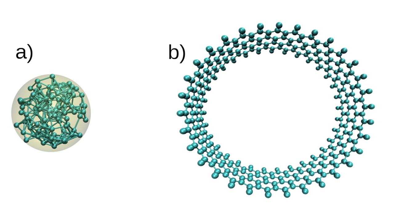
- Construction of Dense CNT Film Models: Researchers built virtual models of dense mesoscale CNT films by combining single-wall carbon nanotubes (SWCNTs) of varying chiralities (which determine metallic or semiconducting properties) and lengths. These models also incorporated regions of amorphous carbon to mimic more realistic material structures.
- Analysis of Network Morphology and Connectivity: Through simulations, the complex interplay between the morphological characteristics of the CNT network (e.g., degree of CNT alignment, average number of contact points, junction density) and the electrical connectivity (formation of percolation pathways) was thoroughly analyzed.
- Identification of Governing Structural Parameters: The modeling identified key structural parameters that govern the electrical current flow within the CNT films. These include the length and alignment of the CNTs, the distribution and quantity of amorphous carbon, and the contact resistance between individual CNTs. It was particularly suggested that CNT length strongly influences the percolation threshold and overall conductivity. Shorter CNTs, for instance, tend to require more junctions, leading to increased contact resistance.
- Impact of Amorphous Carbon: Amorphous carbon, while potentially increasing contact area between CNTs, can also act as an electrical insulator. The study indicated that its distribution and quantity have a complex impact on the film’s overall conductivity.
This mesoscale modeling approach offers a quantitative assessment of how microscopic structures influence macroscopic electrical properties, which is often difficult to achieve through traditional experimental methods alone.
Technical Significance & Outlook
The mesoscale modeling of structure-transport relationships in dense CNT films, especially those containing amorphous carbon, holds significant implications for the design and optimization of CNT films. These insights are crucial for enhancing the performance of CNT-based materials in next-generation transparent conductive films, flexible electronic circuits, sensors, and energy storage devices. Materials scientists and engineers can leverage this modeling tool to more efficiently design CNT films with specific electrical properties, thereby reducing the number of experimental trial-and-error iterations.
The outlook involves further improving the accuracy of the models, including considerations for different types of CNTs (e.g., MWCNTs), doping effects, and responses to various external stimuli (e.g., temperature, strain). Additionally, research will extend to elucidating complex structure-property relationships not only for electrical transport but also for thermal transport and mechanical properties. This mesoscale modeling technology is expected to be a powerful tool for accelerating the practical application of CNT films and driving the development of sustainable, high-performance nanoelectronic materials.


Comments