Key Findings
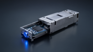
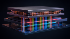
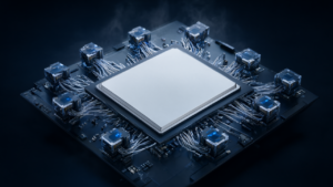
Atomica has introduced its ‘AI Photonic Integration Platform,’ a groundbreaking solution designed to fundamentally resolve the integration bottlenecks prevalent in current artificial intelligence (AI) infrastructure. This innovative platform achieves seamless connectivity between AI accelerators, high-bandwidth memory, and optical input/output (I/O) systems by integrating state-of-the-art microfabrication techniques. This advancement is poised to dramatically enhance the processing capability and efficiency for large-scale AI workloads, thereby accelerating the development of next-generation AI computing systems.
Technical / Clinical Details
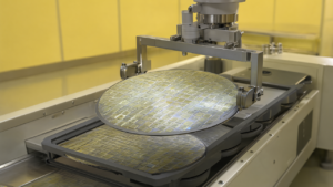
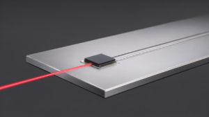
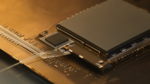
The AI Photonic Integration Platform from Atomica delivers high integration density and performance through a sophisticated combination of microfabrication technologies. It utilizes silicon and glass interposers for high-density connections between diverse chips and components. Through-silicon vias (TSV) and through-glass vias (TGV) facilitate vertical electrical connections, significantly shortening signal paths. Furthermore, advanced re-distribution layers (RDL), wafer-level packaging, and precision bonding techniques are employed to optimize data transmission efficiency between chips. Specialized cavity formation and optical alignment structures ensure efficient coupling with optical fibers, while customer-specific process layers cater to unique application requirements. This integrated platform is specifically engineered to address core challenges in the AI ecosystem, including enhancing AI accelerator performance, strengthening high-bandwidth memory integration, optimizing chiplet packaging efficiency, expanding data center switch capabilities, and accelerating optical I/O speeds.
Background & Context
The rapid evolution of generative AI and large language models has led to increasingly complex AI infrastructures, exacerbating challenges in data transfer and integration. Conventional electrical interconnects are confronting fundamental limits in terms of power consumption, latency, and bandwidth, becoming a critical bottleneck for further improvements in AI computing performance. In this context, photonic integration, leveraging optical technologies, has emerged as a promising solution to overcome these hurdles. Atomica’s platform stands out by integrating various technological elements into a comprehensive solution, simplifying design and manufacturing complexities, and paving the way for improved overall system performance and energy efficiency in AI.
Strategic Significance & Outlook
Atomica’s AI Photonic Integration Platform is set to become a vital tool for AI chip designers, system integrators, and data center operators constructing next-generation AI infrastructure. The platform’s delivery of high bandwidth, low latency, and superior energy efficiency solutions will unlock further AI capabilities, fostering the creation of new applications and services. Particularly, in conjunction with the widespread adoption of chiplet technology, it is expected to accelerate the development of more flexible and high-performance AI hardware, playing a central role in expanding the frontiers of AI. This will likely propel innovation across the AI industry and contribute to its sustainable growth.
Source: https://chiplet-marketplace.com/insights/news/atomica-ai-photonic-integration-platform
Get our weekly technology intelligence — free
Receive an infographic that lets you judge at a glance whether each field’s analysis report is worth reading.
Subscribe Free — Weekly Tech Intelligence
By subscribing, you’ll receive Troy-Technical’s weekly technology intelligence newsletter.
- Your email and selected fields are used only to deliver the newsletter.
- We never share your information with third parties.
- You can unsubscribe anytime via the link in each email.
See our Privacy Policy for details.
Takes about a minute · Unsubscribe anytime