Background and Vulnerabilities in Semiconductor Packaging
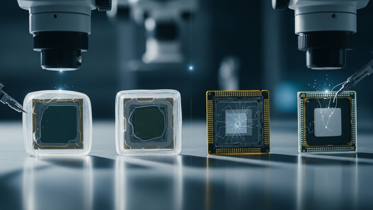
As modern semiconductor devices become smaller, more integrated, and higher performing, their internal dies and interconnects become increasingly vulnerable to physical and thermal stress. Particularly for ultra-thin dies, high-aspect-ratio wire bonds, and advanced packaging structures like System-in-Package (SiP) and Wafer-Level Chip-Scale Packages (WLCSP), even minimal stress generated during manufacturing processes or operating conditions can lead to reduced device reliability and failure. Therefore, the development of low-stress mold compounds to protect these fragile components is indispensable.
Technology and Evolution of Low-Stress Mold Compounds
The latest low-stress Encapsulation Molding Compounds (EMCs) have evolved in material composition and structure to address multiple sources of stress:
- Diversification of Material Composition: While traditional EMCs were primarily epoxy resin-based, new silicone-based compounds and modified epoxy resins incorporating flexible polymer segments have been developed for lower stress. Silicones, with their low elastic modulus and coefficient of thermal expansion (CTE), excel at stress relief during thermal cycling.
- Addressing Stress Sources:
- Thermal Cycling Stress: Stress generated by CTE mismatch between different materials within the package (silicon die, leadframe, mold compound) is effectively managed by the EMC’s internal stress relaxation mechanisms. Optimizing the EMC’s CTE or glass transition temperature (Tg) minimizes thermal stress.
- Moisture-Induced Swelling: To prevent internal stress from EMC swelling due to moisture absorption, materials with low hygroscopicity and additives with excellent moisture barrier properties are introduced.
- Mechanical Stress: EMCs resist mechanical stress from molding pressure during manufacturing processes or external shocks and vibrations with an appropriate balance of hardness and flexibility, protecting internal components.
Technical Significance, Remaining Challenges, and Future Outlook
Low-stress mold compounds are essential technologies for improving the reliability and durability of advanced semiconductor packages. However, further miniaturization of ultra-thin dies, increasing complexity of high-aspect-ratio components, and advancements in heterogeneous integration in SiP and WLCSP continue to pose new challenges. Specifically, there is a demand for material designs that achieve both higher thermal conductivity and lower CTE, polymer synthesis that maintains extremely low elastic modulus while possessing sufficient mechanical strength, and the development of precise stress simulation and management techniques for complex package structures.
In the future, the development of more intelligent packaging materials, such as EMCs with self-healing capabilities or those that can be debonded by specific triggers, could improve the repairability and recyclability of semiconductor devices. These technologies will form the foundation for next-generation high-performance electronics, including AI processors, 5G communications, and IoT devices.


Comments