Background and Challenges in Semiconductor Packaging
Modern semiconductor devices are increasingly integrated and adopting complex 3D packaging structures. In such advanced packaging, mold compounds play a crucial role in protecting devices from external environments and providing mechanical strength. However, inherent stresses generated during the curing and crystallization process of mold compounds can lead to severe problems such as package warpage, delamination between the die and mold, and degradation of the device’s mechanical properties. These challenges are particularly pronounced in large packages and heterogeneous stacked structures, directly affecting product yield and reliability.
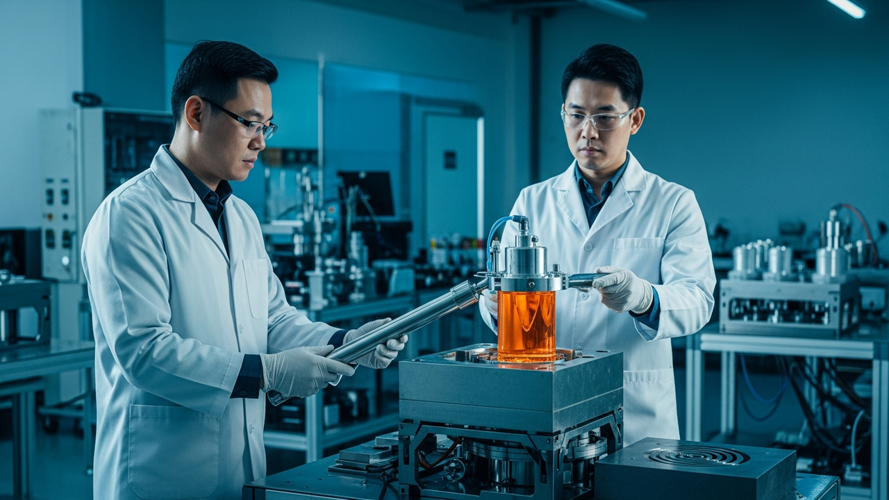
Improvements in Low-Stress Crystallization Techniques
Advanced material manufacturers like Kingfa are focusing on optimizing the crystallization process of mold compounds to resolve these issues. Their approach aims to promote uniform crystal distribution while simultaneously maintaining processing efficiency.
- Advanced Nucleation Systems: Advanced nucleating agents and systems are introduced to control the crystallization process within the mold compound. This ensures uniform crystal formation and growth, reducing imbalances in internal stress. A homogeneous fine-grained crystalline structure improves the material’s mechanical strength and thermal resistance.
- Temperature-Controlled Crystallization Chambers: By using crystallization chambers capable of precise temperature control, a uniform temperature profile is maintained throughout the mold compound. This prevents stress generation due to rapid temperature changes and non-uniform crystallization.
- Modified Injection Parameters: In the injection molding process, parameters such as injection speed, pressure, and mold temperature are optimized to minimize thermal gradients. This ensures uniform filling of the mold compound within the mold and prevents the introduction of non-uniform stresses before crystallization begins.
Technical Significance and Future Outlook
Improvements in low-stress crystallization techniques hold immense technical significance for substantially enhancing the reliability of advanced semiconductor packages. Reduced package warpage and delamination lead to fewer assembly defects in subsequent processes, improving the yield of final products. This is critical for high-value AI processors, High-Performance Computing (HPC) chips, and high-reliability applications like automotive electronics.
In the future, these techniques are expected to evolve further to accommodate more complex package structures (e.g., 3D stacking, chiplet integration) and new materials (e.g., ultra-low CTE substrates). The introduction of real-time crystallization process monitoring and AI-driven optimization techniques is also anticipated. Companies like Kingfa will continue to provide the foundation for sustained growth in the semiconductor industry through these advanced material technologies. The evolution of adhesives and encapsulants is an indispensable factor for realizing next-generation electronics.


Comments