Key Findings
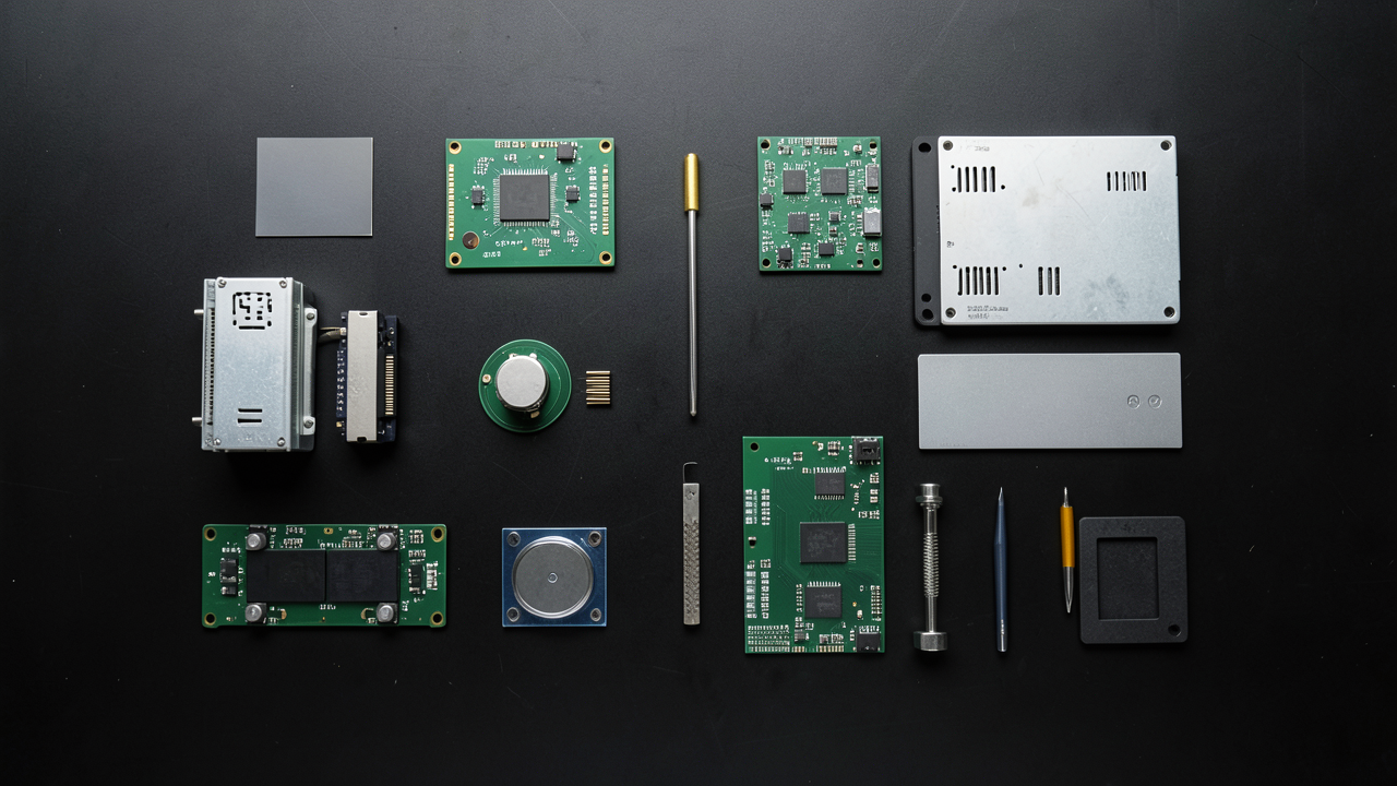
The burgeoning demand for high-performance AI accelerators in data centers has brought to light significant supply chain constraints and fundamental material limitations, particularly the pronounced warpage issues observed in large-scale ABF (Ajinomoto Build-up Film) substrates. To address this critical challenge, leading semiconductor industry players such as TSMC and Ibiden are strategically positioning “glass core substrates” on their technology roadmaps for adoption around 2030. These glass core substrates are anticipated to resolve the limitations of conventional resin core substrates, proving indispensable for enhancing the reliability and performance of increasingly integrated AI semiconductors.
Technical / Clinical Details
ABF substrates utilized in AI accelerators typically comprise a glass-reinforced resin core encapsulated by layers of copper wiring and insulating films, providing both high-density interconnects and a degree of mechanical rigidity. However, as AI chips grow in scale and performance, leading to larger package sizes and increased power consumption, the problem of substrate warpage—driven by differences in coefficients of thermal expansion (CTE)—becomes exacerbated. This warpage directly impacts manufacturing yields during the packaging process and compromises the long-term reliability of the final product. Glass core substrates, in contrast to traditional resin cores, exhibit significantly lower CTE and substantially higher mechanical rigidity. This characteristic enables effective suppression of warpage even in large packages and facilitates the stable formation of high-density wiring. Furthermore, the inherent flatness and uniformity of glass are expected to enable even higher precision in fine wiring patterns and reduce high-frequency signal loss.
Background & Context
The exponential growth of the AI and data center markets has fueled an unprecedented demand for high-performance AI accelerator chips. These chips integrate hundreds of billions of transistors and rely on advanced heterogeneous integration techniques to package multiple dies. This increased density and larger form factor place unprecedented demands on packaging substrates, with thermal management and mechanical stability emerging as critical bottlenecks. While ABF substrates have been the primary choice, their supply capacity and physical limitations are becoming evident. The transition to glass core substrates represents a strategic move to open new frontiers in performance enhancement through packaging technology, especially as the semiconductor industry approaches the limits of Moore’s Law. This is a quintessential example of innovation stemming from the convergence of materials science and semiconductor manufacturing processes.
Strategic Significance & Outlook
The commercialization of glass core substrates is increasingly seen as commencing in 2026, with widespread adoption expected to establish it as a dominant packaging technology in the AI accelerator market by around 2030. While this promises further advancements in AI chip performance and reliability, key challenges ahead include developing advanced glass processing technologies, managing costs, and establishing robust supply chains. Leadership from industry giants like TSMC and Ibiden is expected to accelerate both technological development and mass production. This transformation not only presents significant business opportunities for the semiconductor materials industry but also serves as a foundational technology supporting the evolution of AI, drawing global attention to its trajectory.
Get our weekly technology intelligence — free
Receive an infographic that lets you judge at a glance whether each field’s analysis report is worth reading.
Subscribe Free — Weekly Tech Intelligence
By subscribing, you’ll receive Troy-Technical’s weekly technology intelligence newsletter.
- Your email and selected fields are used only to deliver the newsletter.
- We never share your information with third parties.
- You can unsubscribe anytime via the link in each email.
See our Privacy Policy for details.
Takes about a minute · Unsubscribe anytime







Comments