Key Findings
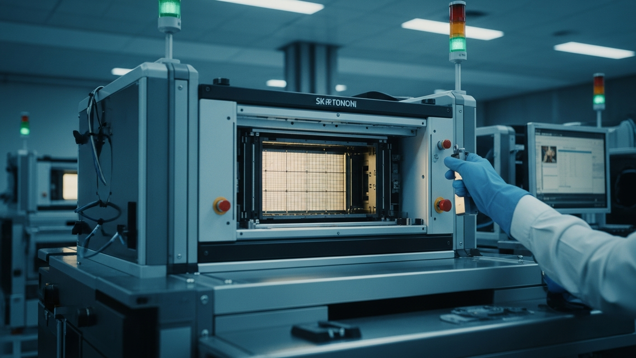
Hanmi Semiconductor has secured a substantial order from SK hynix, valued at ₩44.2 billion (approximately $32 million), for its TC Bonder 4.5 Griffin systems. These advanced thermal compression bonders are essential for the production of SK hynix’s next-generation HBM4 (High Bandwidth Memory), with deliveries expected to commence in early September 2026. This landmark deal highlights the intensified investment in advanced packaging, particularly as the semiconductor industry pivots towards meeting the escalating demands of artificial intelligence workloads.
Technical / Clinical Details
The TC Bonder 4.5 Griffin is a critical piece of equipment in the advanced packaging process, specifically for stacking multiple semiconductor dies with extreme precision. In HBM manufacturing, where numerous DRAM layers are vertically integrated, accurate bonding is paramount for achieving high performance and reliability. Hanmi’s technology addresses the finer pitch and stringent alignment requirements of HBM4, ensuring robust electrical connections and improved thermal dissipation within the stacked memory modules.
Beyond Hanmi’s specific win, the broader advanced packaging equipment market is experiencing robust growth. BE Semiconductor Industries (BESI) reported a remarkable 104.5% year-over-year increase in Q1 2026 orders, totaling €269.7 million. This surge is primarily attributed to the accelerating adoption of hybrid bonding for 2.5D AI-related data center and photonics applications. Similarly, ASMPT is seeing repeat orders for its Chip-to-Substrate (C2S) and Chip-to-Wafer (C2W) TCB solutions, crucial for AI chips and logic chiplets, respectively. These developments indicate that TCB technology, driven by HBM stacking, AI chip C2S, and logic chiplet C2W applications, is a cornerstone for future high-performance computing architectures.
Background & Context
The relentless demand for AI accelerators and high-performance computing (HPC) has shifted the primary bottleneck from front-end wafer fabrication to back-end packaging. Traditional 2D packaging can no longer accommodate the increasing number of transistors and the complex interconnectivity required. This has catalyzed the rapid adoption of 2.5D and 3D packaging technologies, with HBM being a prime example. The precise stacking of memory dies on a logic base, often via interposers, necessitates advanced bonding techniques like TCB.
Industry forecasts by SEMI predict global semiconductor manufacturing equipment sales to reach $145 billion in 2026, primarily fueled by investments in advanced logic, memory, and packaging. This substantial growth underscores the strategic importance of the back-end segment in enabling next-generation silicon. The competitive landscape for HBM, with players like SK hynix, Samsung, and Micron vying for market leadership, directly translates into a strong demand for specialized packaging equipment.
Strategic Significance & Outlook
SK hynix’s procurement of Hanmi Semiconductor’s TC Bonders is a pivotal step towards the mass production of HBM4, which is expected to underpin the next wave of AI and HPC systems. For Hanmi, this order solidifies its position as a critical supplier in the burgeoning HBM ecosystem. The broader trend of escalating TCB and hybrid bonding demand signals a profound transformation in semiconductor manufacturing, where packaging is no longer merely an assembly step but a core technology for performance and power scaling. As chiplet architectures and optical interconnects become more prevalent, the market for advanced packaging equipment will likely continue its upward trajectory, fostering further innovation and investment in this crucial segment of the semiconductor supply chain.
Source: https://www.htx.com/it-it/news/the-iron-rule-of-chip-equipment-is-being-broken-I97homtL
Get our weekly technology intelligence — free
Receive an infographic that lets you judge at a glance whether each field’s analysis report is worth reading.
Subscribe Free — Weekly Tech Intelligence
By subscribing, you’ll receive Troy-Technical’s weekly technology intelligence newsletter.
- Your email and selected fields are used only to deliver the newsletter.
- We never share your information with third parties.
- You can unsubscribe anytime via the link in each email.
See our Privacy Policy for details.
Takes about a minute · Unsubscribe anytime


Comments