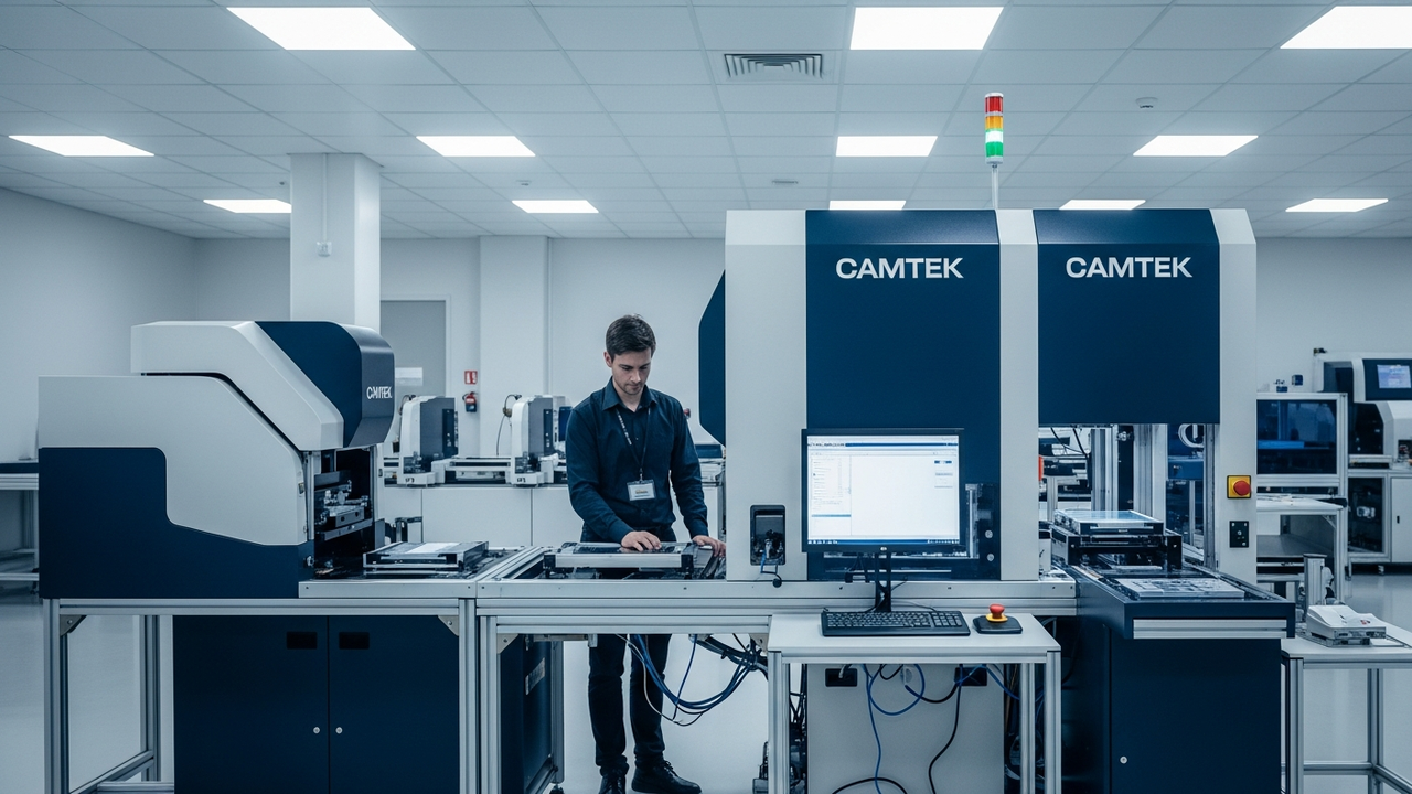
Background: Challenges in Advanced Packaging and the Need for High-Precision Inspection
The relentless evolution of semiconductors, driven by advancements in Artificial Intelligence (AI), High-Performance Computing (HPC), 5G communications, and autonomous driving, has ushered in an era of unprecedented complexity in chip packaging technology. Advanced packaging methods, including 2.5D/3D integration, Wafer-Level Chip-Scale Packaging (WLCSP), and Fan-Out Wafer-Level Packaging (FOWLP), necessitate extremely fine structures and exceptional precision to densely integrate multiple, often dissimilar, chiplets. Consequently, even minute defects or dimensional inaccuracies introduced during the manufacturing process can directly compromise product functionality and lead to significant yield degradation. Thus, high-precision and high-efficiency inspection and metrology solutions are indispensable across the entirety of these intricate packaging processes.
Camtek’s Advanced Inspection and Metrology Platforms
Camtek addresses the critical challenges within the advanced packaging market through its unique suite of 2D and 3D inspection and metrology platforms. These solutions have become widely adopted industry benchmarks, recognized for their outstanding performance and diverse functionalities:
- Sub-Micron Defect Detection: Leveraging cutting-edge optical technology alongside advanced image processing algorithms, Camtek’s systems accurately and efficiently detect minute, sub-micron level defects, including short circuits, opens, foreign material contamination, and bump anomalies.
- CAD-Based Detection Technology: By performing inspections directly against Computer-Aided Design (CAD) data, these systems precisely compare and analyze discrepancies between the fabricated product and its intended design. This capability enables early identification of potential manufacturing issues, fostering a rapid feedback loop crucial during the development phase.
- Inspection for Multi-Layer RDL (Redistribution Layer) Applications: Multi-layer Redistribution Layers (RDLs), foundational for heterogeneous integration, demand extremely fine wiring and precise inter-layer connections. Camtek’s systems accurately inspect defects within these complex multi-layer structures, directly contributing to maintaining high production yields.
- High-Throughput Bump Metrology: Essential for flip-chip and 3D stacking applications, these systems measure the height, diameter, and shape of microscopic bumps (e.g., solder balls or copper pillars) with high speed and precision. This capability is critical for stabilizing bonding quality and enhancing overall device reliability.
These advanced features are indispensable for supporting the relentless trends of miniaturization, increasing complexity, and heterogeneous integration inherent in modern advanced packaging.
Industry Impact and Future Outlook
Camtek’s advanced inspection and metrology solutions empower semiconductor manufacturers to uphold stringent quality and reliability standards in advanced packaging, all while simultaneously boosting production efficiency. For high-performance devices such as AI chips, even marginal improvements in yield can translate into significant gains in cost-efficiency and accelerated time-to-market, underscoring the strategic value of Camtek’s technology. Looking ahead, as packaging technologies continue their rapid evolution—for instance, with innovations like packaging on glass substrates and even more complex chiplet integration schemes—inspection and metrology technologies will similarly need to advance continuously. Camtek is thus positioned to remain a crucial player, supporting the foundational technologies of the next-generation semiconductor industry through continuous innovation in this vital domain.









Comments