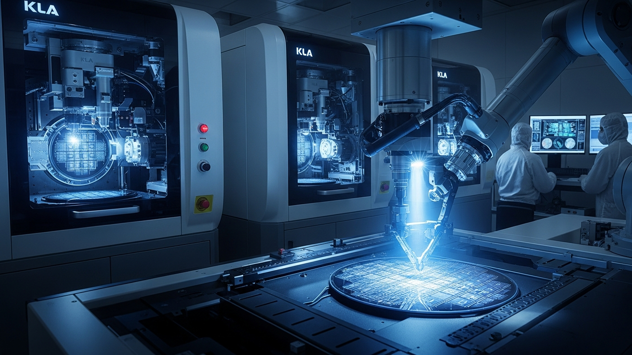
Background: Quality and Yield Challenges in Advanced Packaging
The evolution of technologies such as Artificial Intelligence (AI), High-Performance Computing (HPC), 5G communications, and autonomous driving has dramatically increased the complexity and integration density of semiconductor chips. This necessitates advanced packaging technologies like 2.5D/3D packaging for integrating multiple chiplets, and wafer-level packaging (e.g., WLCSP, FOWLP). However, these intricate processes demand extremely high-precision inspection and metrology, as minute defects or alignment discrepancies can significantly impact the final product’s performance and yield. KLA stands as a leading provider of solutions supporting quality control and efficiency in these advanced packaging processes.
KLA’s Inspection and Metrology Solutions: Technical Features
KLA addresses the diverse challenges of advanced packaging by offering comprehensive process control and enabling solutions across wafer, panel, and component levels. Its portfolio is characterized by the following technical features:
- Comprehensive Inspection Platforms: KLA provides a wide range of inspection systems, including CIRCL™-AP for full-surface inspection and eDR7380™ for e-beam defect review and classification. These systems enable high-precision detection and analysis of sub-micron level defects.
- AI-Powered Process Control: Leveraging AI for inspection data analysis dramatically improves process control and defect analysis. This allows for real-time problem identification and correction, significantly contributing to enhanced manufacturing yields.
- High-Precision Metrology Capabilities: The systems cater to diverse metrology needs, including patterned and unpatterned inspection, overlay metrology, and post-plasma etch/deposition film thickness and profile measurements. Notably, inspection for multi-layer RDL (redistribution layer) applications and high-throughput bump metrology have set industry standards.
- Support for Heterogeneous Integration: As chiplet and dissimilar material integration advances, KLA’s systems provide critical data to ensure high-precision alignment and uniformity, contributing to improved packaging yield and optimized chip performance in complex heterogeneous assemblies.
Industry Impact and Future Outlook
KLA’s advanced packaging inspection and metrology solutions provide the foundational elements for ensuring quality and reliability in the high-volume production of high-performance semiconductors, including AI chips. These technologies empower semiconductor manufacturers to confidently implement more complex and innovative packaging designs, thereby accelerating time-to-market. Especially as AI becomes increasingly sophisticated and chip integration pushes its limits, the evolution of inspection and metrology technologies like those from KLA is an indispensable factor supporting the overall advancement of the semiconductor industry. Further automation and intelligence through AI are expected to enhance the efficiency and precision of packaging processes in future smart factories.









Comments