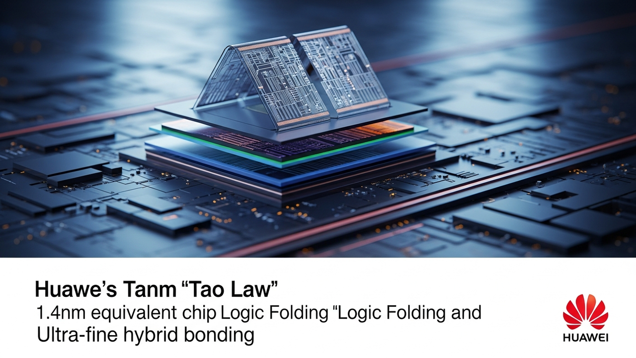
Concepts of “Tao Law” and “Logic Folding”
Huawei’s proposed “Tao Law” represents a novel scaling approach for semiconductor processes, envisioning an alternative to traditional Moore’s Law. It aims to enhance effective chip density not only by scaling down transistor sizes on a single plane but also by extending chips vertically. Central to this strategy is an innovative methodology called “Logic Folding.” Logic Folding involves distributing logic gates across multiple vertically stacked active layers instead of confining them to a single silicon layer. This allows for the physical integration of more transistors within the same footprint, effectively delivering performance gains comparable to advanced process node scaling. This approach holds the potential to overcome the physical and economic limitations currently challenging conventional miniaturization techniques.
Role of Ultra-Fine Hybrid Bonding and TSV Technology
The realization of Logic Folding critically depends on highly advanced chip stacking and interconnection technologies. Huawei places ultra-fine-pitch hybrid bonding and Through-Silicon Via (TSV) technology at the core of this endeavor. Hybrid bonding enables direct copper-to-copper connections between chips, achieving significantly finer connection pitches than conventional micro-bumps. This maximizes data transfer speed and efficiency between vertically stacked logic layers. The Kirin 2026 has already demonstrated a groundbreaking hybrid bonding pitch of 1.5μm, showcasing the maturity of this technology.
Next-Generation Mobile SoC and Market Implications
Huawei plans to launch a mobile System-on-Chip (SoC) utilizing this “Tao Law” and Logic Folding technology in autumn 2026. This new chip aims to achieve a 55% increase in effective transistor density compared to traditional designs, which is expected to dramatically enhance the performance of smartphones and other mobile devices. The successful implementation of Logic Folding necessitates significant advancements in Electronic Design Automation (EDA) toolchains, enabling them to treat multiple stacked dies as a single, continuous design entity. Huawei’s move demonstrates the strong resolve of the Chinese semiconductor industry to pursue performance gains through innovative packaging technologies, even with limited access to leading-edge foundries due to U.S. export restrictions. This strategy has the potential to introduce a new direction for the global semiconductor roadmap.
Source: https://leonliao.substack.com/p/tau-scaling-law-vs-moores-law-from


Comments