Background and Challenges in Semiconductor Packaging
High-power semiconductor devices, particularly for power electronics and high-density ICs in data centers, must withstand high operating temperatures and frequent thermal cycling. In these harsh environments, significant thermal stress is generated in the die attach material bonding the die to the substrate, with crack initiation and propagation being a primary cause of device failure. While conventional lead-free solder alloys have been widely adopted due to environmental regulations, their resistance to thermal cycling fatigue has been a persistent challenge. Consequently, there has been a demand for next-generation die attach materials that offer higher reliability and extended lifespan.
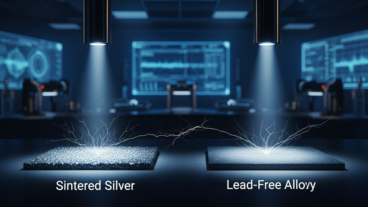
Technical Innovation of Sintered Silver and Crack Propagation Resistance
Indium Corporation has reported that its sintered silver die attach materials exhibit remarkably superior crack propagation resistance compared to traditional lead-free alloys. The core of this technology lies in its unique microstructure and the resulting energy absorption mechanisms:
- Porous Microstructure: Sintered silver materials consist of fine silver particles bonded by heat and pressure, forming a controlled porous structure internally. This porous structure alleviates stress concentration at crack tips and irregularly deflects crack paths as they propagate through the material, significantly reducing propagation velocity.
- Energy Absorption Mechanism: As a crack navigates through the porous structure, energy dissipation occurs at micro-voids and interfaces, enhancing the material’s overall resistance to crack propagation. This effectively slows down actual crack growth, akin to impeding its path through a maze.
- Experimental Results: Laboratory power cycling tests demonstrated that sintered silver reduced crack growth rates by 60-70% compared to standard SAC (Sn-Ag-Cu) lead-free solder alloys. This implies a dramatic extension of device thermal cycling life.
Technical Significance and Future Outlook
The superior crack propagation resistance of sintered silver die attach materials holds immense technical significance for high-reliability semiconductor packaging. It will substantially contribute to extending the lifespan and improving the reliability of devices in applications demanding high power density and harsh operating environments, such as EV power modules, 5G communication infrastructure, AI processors, and aerospace electronics. By being lead-free while exceeding the performance limitations of conventional lead-free solders, it satisfies both environmental regulations and high-performance requirements. Moving forward, sintered silver technology is expected to see accelerated adoption in a broader range of semiconductor packaging applications through further material design optimization, manufacturing process efficiencies, and cost reductions. Furthermore, given its excellent thermal dissipation properties, sintered silver is also gaining attention as a next-generation thermal management solution.
Source: https://eureka.patsnap.com/report-sintered-silver-vs-lead-free-alloys-crack-propagation-rates


Comments