Key Findings
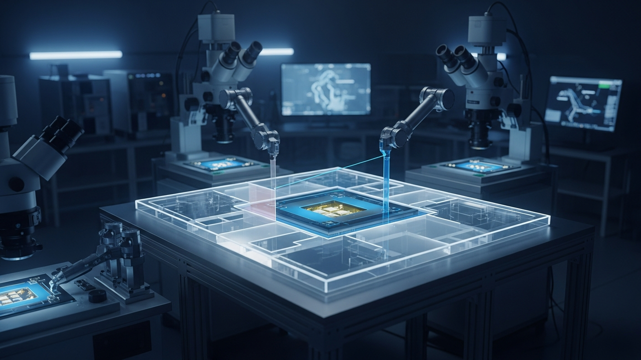
A recent PatSnap Eureka report highlights that minimizing voiding in chip embedding epoxies is a critical reliability challenge in high-performance electronic packaging, especially for demanding automotive and aerospace systems. Voids can significantly degrade device reliability, making their suppression a central focus of technological innovation.
Technical / Clinical Details
The primary approaches to reducing void formation involve both material and process advancements. On the material front, leading companies such as Resonac (formerly Showa Denko Materials) and Sumitomo Bakelite are focusing on developing advanced epoxy molding compounds (EMCs) with optimized properties:
- Optimized Rheological Properties: Precisely controlled resin flow ensures uniform filling of micro-gaps and complex structures, suppressing void entrapment.
- Controlled Curing Kinetics: Rapid curing can trap bubbles, so precise control over curing speed and profile allows sufficient time for bubbles to escape.
- Low-Viscosity Formulations: Lower viscosity epoxies wet around chips more efficiently and promote bubble expulsion.
- Degassing Additives: Specialized additives are incorporated to efficiently release gases generated during curing, preventing void formation.
On the process front, techniques like vacuum molding, dispensing under reduced pressure, and optimized thermal curing profiles are employed. These technologies aim to improve adhesive wetting, ensure dimensional stability, and enhance the long-term reliability of devices.
Background & Context
Modern electronic devices demand miniaturization, higher integration, and enhanced reliability at elevated operating temperatures. In automotive electronics and aerospace applications, safety and reliability are paramount, as even minor voids can lead to short circuits, reduced heat dissipation, mechanical weak points, and ultimately, device failure. Consequently, packaging material manufacturers are heavily investing in developing void-free or near-voidless epoxy resins. This technology is also indispensable for the advancement of AI chips and High-Performance Computing (HPC), providing a key solution to packaging challenges in complex chip designs.
Strategic Significance & Outlook
Advances in void reduction technologies for chip embedding epoxies are essential for the development of next-generation high-reliability electronic devices. These advancements will enable more robust and longer-lasting devices, leading to increased adoption in critical applications such as autonomous vehicles, space probes, and medical implants, where human safety may be involved. Going forward, material suppliers and device manufacturers are expected to leverage AI-driven material design and process optimization to further suppress void formation, accelerating technological innovation across the electronics industry.


Comments