Key Findings
A recent PatSnap Eureka report highlights the accelerating adoption of UV-curable adhesives in chip embedding operations within the semiconductor industry. This trend is primarily driven by the superior rapid curing capabilities and significant advantages these adhesives offer in precision manufacturing, leading to dramatic improvements in production efficiency and throughput.
Technical / Clinical Details
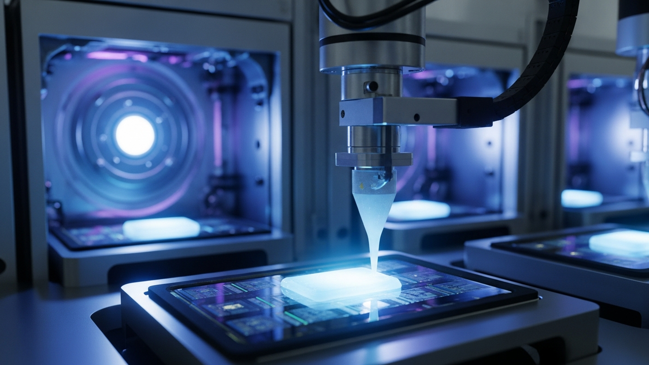
UV-curable adhesives initiate and complete curing within seconds when exposed to specific wavelengths of ultraviolet (UV) light. According to the report, these adhesives typically cure within 5-30 seconds, with some ultra-fast curing types achieving initial tack in just 2-3 seconds. This represents a substantial reduction in manufacturing cycle time compared to traditional thermosetting adhesives, which can take minutes to hours. Leading material manufacturers, such as 3M, are developing UV-curable adhesives based on advanced acrylate chemistry, focusing on achieving multi-functional performance including structural bonding, thermal management, electrical insulation, and low shrinkage. Low shrinkage is essential for minimizing material volume change during curing, thereby ensuring dimensional stability of precision components. These adhesives also demonstrate excellent adhesion strength to various substrates commonly used in semiconductor packaging (e.g., silicon, ceramics, polymers), enhancing device reliability. Furthermore, being solvent-free, they emit no VOCs (Volatile Organic Compounds), contributing to improved workplace safety and environmental compatibility.
Background & Context
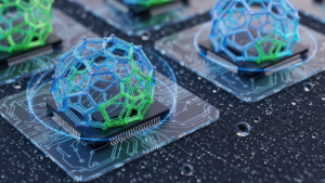
In the semiconductor industry, as Moore’s Law approaches its limits, innovative packaging technologies are indispensable for achieving both miniaturization and enhanced performance. Chip embedding, a technique where chips are directly integrated into the substrate, enables thinner packages, reduced footprints, and improved electrical characteristics. This process demands fast and high-precision bonding, where traditional adhesive technologies could become a production bottleneck. UV-curable adhesives, with their rapid curing and precise application and curing control capabilities, are emerging as an ideal solution to this challenge, directly contributing to the advancement of AI chips, HPC (High-Performance Computing), and mobile devices.
Strategic Significance & Outlook
The continued advancement of UV-curable adhesive technology will play a crucial role in the future of semiconductor packaging. Faster and more reliable bonding solutions will enable the mass production of next-generation compact and highly integrated devices, accelerating the widespread adoption of cutting-edge technologies like AI, 5G, IoT, and autonomous vehicles. Moving forward, material manufacturers are expected to focus on developing custom formulations that offer even better thermal management performance, mechanical strength, and specific application requirements (e.g., flexibility or impact resistance). Optimizing and integrating UV curing processes will also be an important direction for improving productivity.


Comments