Key Findings
Applied Materials has revised its 2026 forecast for advanced packaging revenue, projecting an increase of over 70% year-over-year, driven by robust investments in AI semiconductors. This represents a substantial 20-percentage-point upward revision from its prior forecast of over 50% growth, announced just three months earlier. This acceleration is fueled not only by front-end miniaturization for AI semiconductors but also by surging investments in High-Bandwidth Memory (HBM) and 3D packaging, which connects multiple dies. To capitalize on this expanded market opportunity, Applied Materials has introduced a suite of six new systems for DRAM and advanced packaging, including the Nokota™ VMax™ 2 ECD system, Centura Prime Epi, Producer Avila 2 PECVD, Opta Quad CMP, VeritySEM 7AP, and SEMVision G7AP.
Technical Details
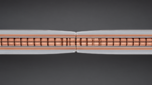
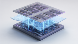
Modern AI processors are increasingly limited by the data transfer speed between computing and memory. Advanced packaging overcomes this bottleneck by bringing compute and memory closer together, thereby accelerating data transfer and improving energy efficiency. Applied Materials’ newly unveiled Nokota™ VMax™ 2 ECD system is an electroplating deposition (ECD) tool specifically engineered to meet the complex demands of HBM packaging. ECD is a critical process for forming ultra-fine copper interconnects and via fills, essential for creating high-density interconnections within HBM stacks. Furthermore, Applied Materials leverages its existing front-end technologies, adapting them to provide a comprehensive range of process solutions—including etching, thin-film deposition, Chemical Mechanical Planarization (CMP), and inspection & metrology—that enhance yield in DRAM manufacturing and advanced packaging. The 52% year-over-year increase in DRAM revenue, inclusive of HBM packaging, during Q3 FY2026 underscores the direct impact of surging AI accelerator demand on the memory market.
Background & Context
The rapid evolution of AI is driving a structural transformation across the semiconductor industry, establishing advanced back-end packaging as a primary driver for performance enhancement, beyond conventional front-end process miniaturization. Heterogeneous integration approaches, such as HBM and 2.5D/3D chip stacking, dramatically boost AI chip performance but also increase manufacturing complexity and cost. Applied Materials, as a leading semiconductor equipment manufacturer, focusing on advanced packaging and expanding its product portfolio, confirms that this market growth is a long-term trend rather than a temporary surge. The company views this escalating demand as an opportunity to broaden the applicability of its existing technologies and is actively pursuing strategies to capture the rising adoption of HBM and 3D packaging.
Strategic Significance & Outlook
Applied Materials’ strong growth projections and new product introductions indicate that the advanced packaging market will continue to expand in tandem with AI technology advancements. The further proliferation of HBM and 3D packaging technologies will introduce more intricate package structures and stringent yield requirements, making ongoing innovation in inspection & metrology, process control, and materials technology critically important. By swiftly adapting to these market shifts, Applied Materials is poised to further solidify its position as a central supplier within the AI-era semiconductor ecosystem. Its technologies are expected to play an increasingly vital role, particularly in data center and edge computing sectors demanding high-performance AI chips.
Source: https://xenospectrum.com/en/applied-materials-packaging-growth/
Get our weekly technology intelligence — free
Receive an infographic that lets you judge at a glance whether each field’s analysis report is worth reading.
Subscribe Free — Weekly Tech Intelligence
By subscribing, you’ll receive Troy-Technical’s weekly technology intelligence newsletter.
- Your email and selected fields are used only to deliver the newsletter.
- We never share your information with third parties.
- You can unsubscribe anytime via the link in each email.
See our Privacy Policy for details.
Takes about a minute · Unsubscribe anytime