Key Findings
The semiconductor inspection equipment market is projected to expand at a Compound Annual Growth Rate (CAGR) of 7.9% from 2026 to 2034, reaching a market value of $13.4 billion by 2034. This growth is primarily fueled by the increasing complexity of AI chips and the rapid adoption of advanced packaging technologies. KLA is a frontrunner in advanced packaging process control, reporting approximately 70% year-over-year revenue growth in this segment, indicating that back-end and mid-end inspection are becoming independent budget items for OEMs and fab operators. Testing and metrology for AI chips are no longer confined to final production pass/fail decisions; they now play a strategic role in determining yield, reliability, and supply chain competitiveness.
Technical Details
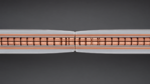
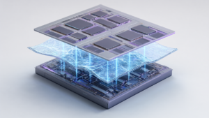
Advanced packaging techniques such as hybrid bonding, fan-out wafer-level packaging, and 2.5D/3D chip stacking necessitate the inspection of bonding pads at extremely fine pitches, often as small as 1–2 micrometers. To address these stringent requirements, advanced inspection tools—including X-ray Computed Tomography (CT), Scanning Acoustic Microscopy (SAM), and 3D optical profiling tools—are being adopted, extending beyond the capabilities of traditional front-end inspection suites. These technologies are crucial for non-destructively detecting hidden defects within interconnects, redistribution layers (RDLs), vias, and interfaces. Companies like Applied Materials and Onto Innovation also offer process control solutions that combine optical inspection, electron-beam inspection, defect review, metrology, data analytics, and AI-based approaches to enhance yield management and process optimization. KLA Corporation, in particular, stands as one of the most significant global suppliers with comprehensive capabilities spanning optical inspection, e-beam inspection, defect review, metrology, and process control analysis.
Background & Context
The evolution of AI and High-Performance Computing (HPC) applications is accelerating the shift towards larger, denser, and higher-value advanced packages, including emerging glass panel substrate technologies. With this increasing package complexity, reliability risks often arise from hidden defects within interconnections, RDLs, vias, and interfaces—defects that are difficult to access through optical inspection or electrical pass/fail tests alone. Terry Tsao, Global CMO and President of SEMI Taiwan, emphasizes that as AI chip value and complexity grow, testing and metrology become increasingly indispensable for determining yield, managing costs, and enabling efficient mass production. KLA is projected to reach $1 billion in revenue from its advanced packaging process control business in fiscal year 2026, solidifying its market position.
Strategic Significance & Outlook
The continued growth of the semiconductor inspection equipment market reflects the escalating need for quality and reliability in AI-era semiconductor manufacturing. The adoption of advanced techniques like X-ray CT and SAM is expected to expand, with further advancements in real-time, in-line inspection capabilities. Moreover, inspection systems are increasingly integrating AI and data analytics to improve the accuracy of defect classification and streamline process optimization. This enables chip manufacturers to identify issues more rapidly, implement corrective actions, and mitigate the rising production costs associated with advanced packaging complexity, ultimately reducing time-to-market. In the future, inspection and metrology technologies are poised to be recognized as one of the most strategic elements in AI semiconductor manufacturing.
Get our weekly technology intelligence — free
Receive an infographic that lets you judge at a glance whether each field’s analysis report is worth reading.
Subscribe Free — Weekly Tech Intelligence
By subscribing, you’ll receive Troy-Technical’s weekly technology intelligence newsletter.
- Your email and selected fields are used only to deliver the newsletter.
- We never share your information with third parties.
- You can unsubscribe anytime via the link in each email.
See our Privacy Policy for details.
Takes about a minute · Unsubscribe anytime