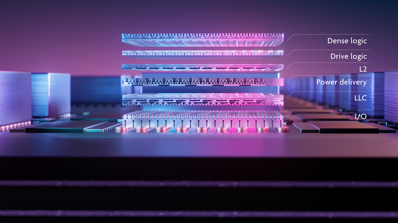
The Imperative for High-Density Integration
In the vanguard of high-performance semiconductors, particularly for demanding applications like AI accelerators and data center processors, maximizing chip-to-chip connection density while concurrently minimizing data transmission latency and power consumption represents a critical challenge. To address this imperative, 3D integration — the vertical stacking of chips — has emerged as a cornerstone architectural strategy. Among its diverse methodologies, hybrid bonding distinguishes itself as a frontrunner, enabling direct, high-density copper-to-copper interconnects between stacked tiers. Transcending the scaling limitations of traditional micro-bump bonding to achieve ever-finer interconnect pitches is pivotal for unlocking future performance frontiers.
Breakthrough: 200nm Pitch Hybrid Bonding
Imec and EV Group (EVG) have announced a groundbreaking advancement in this critical field. Unveiled at ECTC 2026, their collaborative research successfully demonstrated wafer-to-wafer hybrid bonding on 300mm wafers with an extraordinarily fine copper interconnect pad pitch of just 200 nanometers. This achievement not only sets a new industry benchmark but significantly surpasses existing records for interconnect density. Crucially, the post-bond overlay vector was achieved with remarkable accuracy, remaining consistently below 40 nanometers across the entire 300mm wafer. This level of precision is paramount for guaranteeing the robustness, reliability, and optimal electrical performance of the interconnected structures. This unprecedented feat was enabled by meticulous co-optimization of the entire process flow, including the strategic use of SiCN as a high-performance dielectric material and a precisely controlled chemical mechanical polishing (CMP) step meticulously engineered prior to the bonding process.
Technical Significance and Future Outlook
The successful demonstration of 200nm pitch hybrid bonding is poised to profoundly impact the architectural landscape of next-generation computing. It unlocks the capability for unprecedented high-density interconnects in vertically stacked logic-to-logic and memory-to-logic tiers. This breakthrough is expected to dramatically alleviate data transmission bottlenecks, consequently boosting the performance of demanding AI and High-Performance Computing (HPC) applications. This technology will accelerate the realization of advanced chiplet-based designs and sophisticated 3D-ICs, further cementing hybrid bonding’s pivotal role in the broader semiconductor industry roadmap. Looking ahead, it is anticipated to serve as a fundamental enabling technology for engineering more functional, compact, and energy-efficient devices across various domains.


Comments