New Technology– category –
-

NASA Announces Artemis III Crew for 2027 Earth Orbit Mission: Accelerating Human Return to Moon with HLS Lander Tests
NASA USA Overview NASA announced the crew for the Artemis III mission in 2027, comprising Commander Randy Bresnik, Pilot Luca Parmitano, and Mission Specialists Frank Rubio and Andre Douglas. The mission's primary objective is to demonst... -
TSMC’s COUPE Platform for Co-Packaged Optics Targets 2026 Mass Production, Integrating Micro LEDs for AI Cluster Performance Boost
The Storm Media Taiwan Overview TSMC has announced the 2026 mass production launch of "COUPE" (Compact Universal Photonic Engine), an innovative platform for co-packaged optics (CPO) interconnects. Utilizing SoIC bonding to stack photoni... -
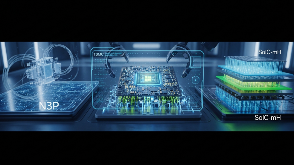
Apple’s M5 Ultra Pioneers Integration with TSMC’s N3P Process and SoIC-mH Packaging
TrendForce Taiwan Overview Reports indicate Apple's upcoming M5 Ultra chip, expected at WWDC, will likely leverage TSMC's N3P process node and its advanced SoIC-mH (System-on-Integrated-Chips – molded horizontal packaging) technology. So... -
Intel and Tesla Partner on AI6 Data Centers, Tapping Advanced Packaging for Production at Austin’s ‘Terafab’
Jamie's Substack USA Overview Tesla has announced a strategic partnership with Intel Foundry Services to scale its AI6 chip-powered data center clusters, extensively utilizing Intel's advanced packaging technologies. The collaboration wi... -
Advanced Packaging’s Evolution: 2.5D/3D Integration, Chiplets, and Hybrid Bonding Propel AI and HPC
Springer Professional Germany Overview Semiconductor packaging technology has dramatically evolved from 2D to 2.5D and 3D IC integration, a transformation accelerated by the explosive demand from AI and High-Performance Computing (HPC). ... -
Sub-10nm Residual Distortion Achieved in Low-Distortion Fusion Bonding with Pneumatically Curved Wafers for Advanced Semiconductors
arXiv USA Overview A recent arXiv publication reports the development of a novel low-distortion fusion bonding technique that employs pneumatically curved wafers to achieve an exceptionally low residual grid distortion of less than 10 na... -
Europe Boosts Investment in Advanced Packaging and Chiplet Integration; imec’s FAMES Pilot Line Aims to Mitigate Regional Supply Chain Risks
Astute Group UK Overview Europe is significantly increasing investment in advanced packaging and chiplet integration technologies to diversify its semiconductor supply chain and reduce regional procurement risks, shifting focus from pure... -
Samsung to Establish Gwangju Advanced Packaging Facility, Eyes Full HBM Hybrid Bonding Transition by 2029
TrendForce South Korea Overview Samsung Electronics is reportedly considering a new advanced semiconductor packaging plant in Gwangju, South Korea, with investment plans potentially announced by June 2026. This strategic facility will fo... -
TSMC to Boost CoWoS Capacity Tenfold to 130K Wafers/Month by Late 2026, Accelerates Glass-Substrate CoPoS for AI Chips
Tom's Hardware USA Overview TSMC is aggressively expanding its advanced packaging capacity, projecting a tenfold increase in CoWoS production to over 130,000 wafers per month by the end of 2026 to meet surging AI demand. Despite this, de... -
Reliability of AI Antibody Design Hinges on Training Data: AlphaFold Era Highlights Data Quality Challenge
Drug Discovery News USA Overview Advancements in protein AI, such as AlphaFold, have ushered in a new computational era for antibody discovery, enabling predictions of protein folding and interactions with near-experimental accuracy. How...