Key Findings
Fraunhofer IPMS has successfully developed high-density chiplet systems at the wafer level. This innovative approach aims to dramatically increase chip integration density for artificial intelligence (AI) and high-performance computing (HPC) applications, paving new avenues for next-generation AI hardware design.
Technical Details
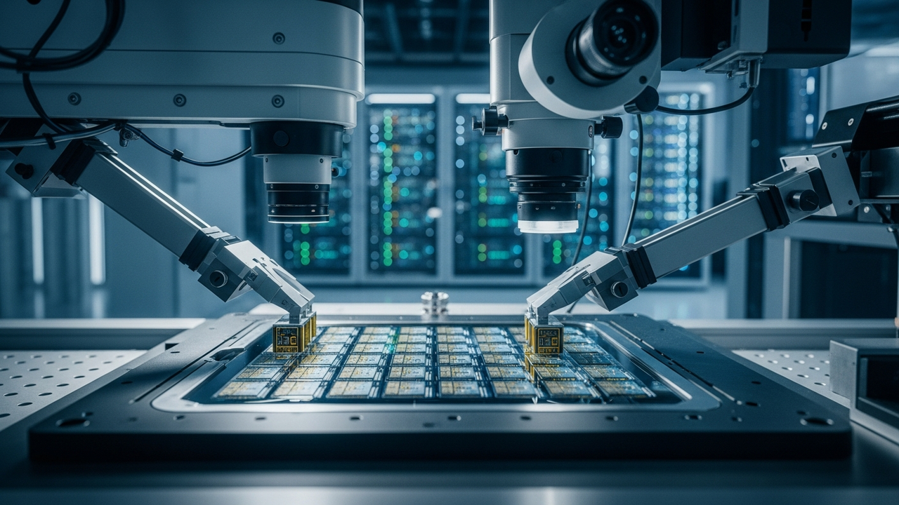
The high-density chiplet systems developed by Fraunhofer IPMS achieve significantly higher integration density than traditional chip integration methods by combining fine interconnect technology with advanced 3D stacking techniques. Wafer-level integration minimizes the connection distance between chiplets, substantially reducing signal latency and power consumption. This technology proves particularly effective in applications demanding immense data processing capabilities and high-speed communication, such as AI accelerators and large-scale multi-core processors. It also synergizes with hybrid bonding technology, which enables ultra-fine-pitch inter-die connections, maximizing the performance and efficiency of AI chips.
Background and Context
With the deceleration of Moore’s Law, the semiconductor industry is increasingly looking beyond miniaturization to advanced packaging and chiplet technologies for performance improvements. The explosive growth of AI has accelerated this trend, creating a strong demand for high-density, high-bandwidth, and low-power solutions. Chiplets offer the potential to increase design flexibility and reduce manufacturing costs by integrating multiple dies with different functionalities, but their realization requires highly precise integration technologies. Fraunhofer IPMS’s research strengthens European technological leadership in this field and represents a significant contribution to the global AI supply chain.
Strategic Significance and Outlook
The high-density chiplet systems developed by Fraunhofer IPMS will be indispensable technologies for next-generation AI and HPC systems. Wafer-level integration offers significant advantages in terms of scalability and cost-efficiency, enabling the development of smaller and more powerful AI chips. As this technology progresses towards commercialization, it is expected to enhance the performance and efficiency of a wide range of AI applications, from data centers to edge devices, fostering further adoption and evolution of AI technology. This marks an important achievement that drives a new wave of innovation in the semiconductor industry.


Comments