Key Findings
Samsung is reportedly poised to launch a physical AI chiplet platform as early as next year. This initiative aims to accelerate the development of next-generation chips specifically designed for AI inference and infrastructure, providing crucial enhancements in high bandwidth and energy efficiency to meet the explosive demand for artificial intelligence (AI).
Technical Details
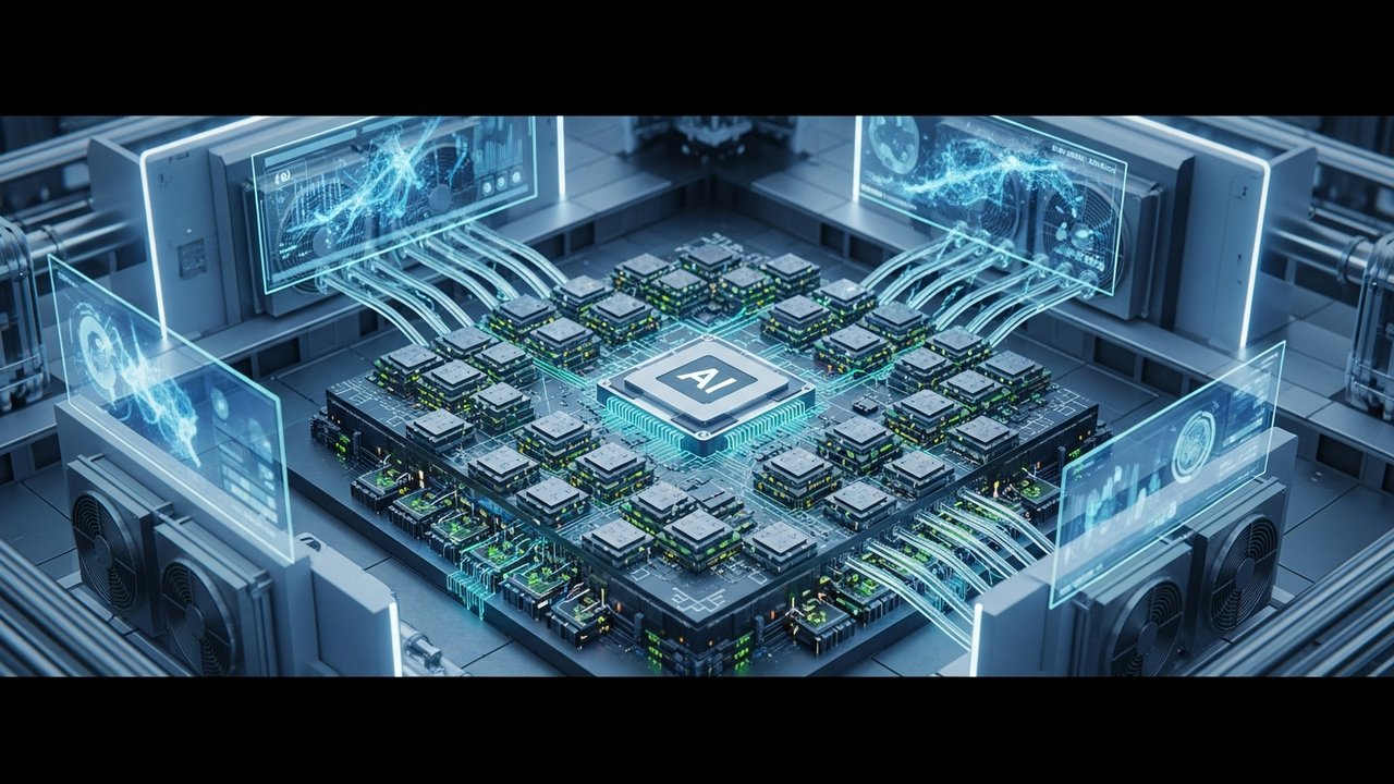
This physical AI chiplet platform will be central to Samsung’s strategy of achieving system-level co-optimization within an integrated development framework that encompasses advanced logic, memory, and packaging. The chiplet architecture aims to enhance design flexibility and surpass performance limitations of monolithic chips by integrating multiple dies with different functionalities. Particularly in next-generation HBM (High-Bandwidth Memory) architectures, leveraging advanced logic nodes in the base die improves power efficiency and boosts data throughput. As I/O density continues to scale, optimizing the base die becomes a critical factor in enhancing overall system efficiency. Samsung Foundry’s 2.xD Cube Packaging enables heterogeneous integration of multiple chips, achieving both high-density integration and high bandwidth.
Background and Context
The rapid evolution of AI presents new challenges and opportunities for the semiconductor industry. Training and inference of large-scale AI models require immense computational power and memory bandwidth, which traditional monolithic chip designs are increasingly struggling to meet. Chiplet technology has emerged as a promising solution to this challenge, and its adoption is accelerating across the industry. Electronic Design Automation (EDA) companies like Cadence and Synopsys are also deepening their collaboration with Samsung Foundry, offering solutions to improve power and performance for AI and multi-die designs using 2nm processes and 3D-IC technology, indicating a clear industry-wide shift towards chiplet-based architectures.
Strategic Significance and Outlook
The launch of Samsung’s physical AI chiplet platform will significantly bolster its competitiveness in the AI semiconductor market. This platform is expected to provide faster and more energy-efficient solutions, particularly for AI inference, improving the performance of a wide range of applications from edge AI to data centers. Samsung’s continued investment in advanced packaging and chiplet technologies is anticipated to be a crucial step in pushing the limits of AI-era computing capabilities and contributing to the construction of sustainable AI infrastructure.


Comments