Key Findings
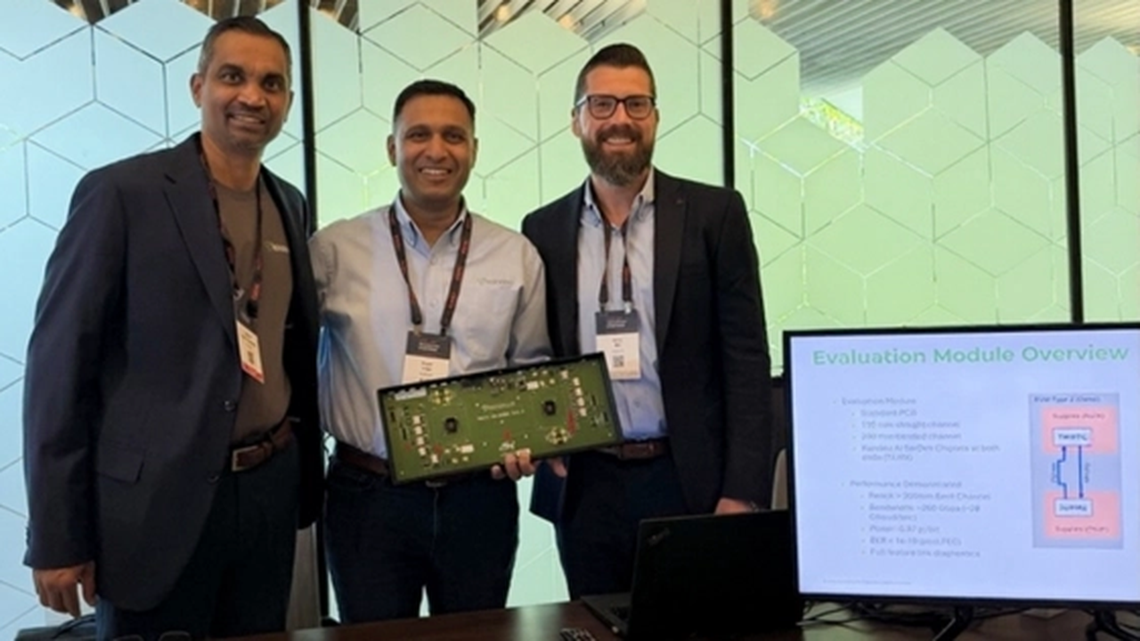
Synopsys announced at SAFE Forum 2026 its new solutions designed to dramatically improve power efficiency and performance for artificial intelligence (AI) and multi-die designs, utilizing Samsung Foundry’s latest process technologies. This innovative approach directly addresses the surging demand for AI infrastructure and physical AI, aiming to accelerate high-performance computing solutions for next-generation AI systems.
Technical Details
The solutions introduced by Synopsys include optimized Electronic Design Automation (EDA) tools and Intellectual Property (IP) portfolios for Samsung Foundry’s advanced processes, particularly for cutting-edge nodes like 2nm. This enables designers to minimize power consumption while maximizing processing speed in logic, memory, and interconnect designs for AI chips and multi-die systems. Specifically, by collaborating with advanced packaging technologies such as Samsung’s 2.xD Cube Packaging, heterogeneous integration of multiple chips can be performed efficiently, leading to significant improvements in overall system bandwidth and energy efficiency. This is a critical factor in AI design, where system-level co-optimization becomes indispensable as I/O density continues to scale.
Background and Context
The explosive growth of AI presents unprecedented design challenges for the semiconductor industry. Traditional monolithic chip designs are finding it difficult to balance the immense computational power, data bandwidth, and low power consumption required by AI workloads. Chiplet and 3D-IC (3-Dimensional Integrated Circuit) technologies have emerged as primary solutions to this challenge, necessitating close collaboration between semiconductor manufacturers and EDA vendors. Cadence is also deepening its collaboration with Samsung Foundry on 2nm and 3D-IC technologies, providing solutions to improve power and performance for AI and multi-die designs, which further indicates the industry-wide acceleration towards building ecosystems for next-generation AI systems.
Strategic Significance and Outlook
The collaboration between Synopsys and Samsung Foundry is crucial for accelerating innovation in the AI and HPC markets. The combination of optimized EDA solutions and advanced process technologies will shorten AI chip design cycles and time-to-market, while enabling the development of higher-performance and more energy-efficient AI processors. This initiative is expected to be an indispensable factor in supporting the continuous evolution of AI infrastructure and shaping a future where physical AI proliferates across autonomous driving, robotics, smart cities, and beyond.


Comments