June 2026– date –
-

Applied Materials Achieves Record $7.91 Billion Revenue in Q2 2026, Advanced Packaging Business to Accelerate Over 50% for AI
MLQ.ai USA Overview Applied Materials reported record revenue of $7.91 billion in Q2 2026, marking a 13% sequential and 11% year-over-year increase, with non-GAAP gross margin reaching 50%, an 80 basis point improvement. The company anti... -
AMD Announces Over $10 Billion Taiwan Ecosystem Investment to Bolster AI Infrastructure and Advanced Packaging Manufacturing
Electronics Engineering Herald - EEHerald USA Overview AMD announced an investment exceeding $10 billion in Taiwan's ecosystem to expand its AI infrastructure and advanced packaging manufacturing capabilities. This significant capital in... -
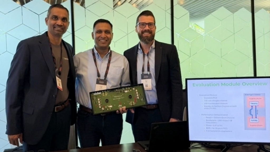
CEA-Leti Demonstrates 1µm Pitch Die-to-Wafer Hybrid Bonding, Addressing AI Hardware Bottlenecks
Chiplet Marketplace France Overview CEA-Leti announced a significant advancement at ECTC 2026, demonstrating functional test vehicles utilizing die-to-wafer (D2W) hybrid bonding down to 1µm pitch, poised to resolve critical AI hardware b... -
Intel to Build $3.3 Billion Glass Core Substrate Manufacturing Facility in India to Bolster Advanced Packaging Supply
TrendForce USA Overview Intel, in collaboration with 3D Glass Solutions (3DGS), is progressing with plans to invest approximately $3.3 billion in an advanced packaging glass core substrate manufacturing facility in Odisha, India. The pla... -
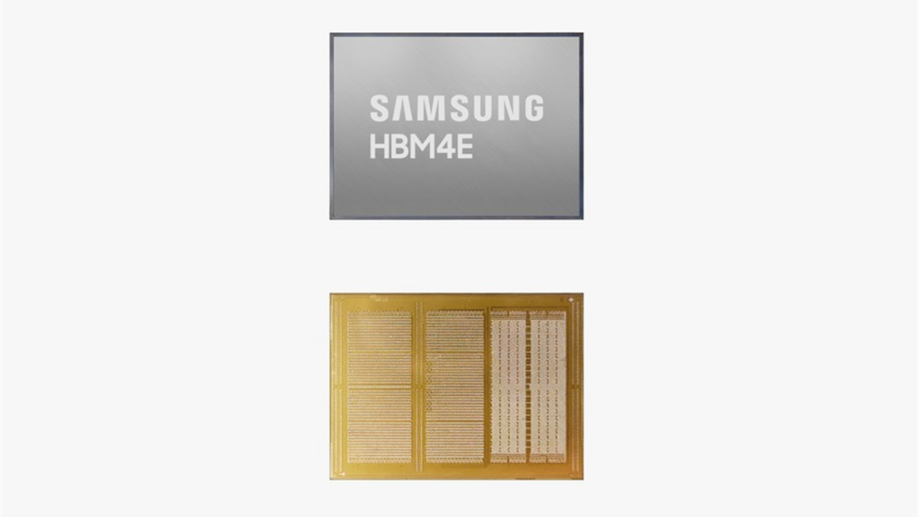
Samsung Electronics Begins Shipment of Industry’s First 12-Layer HBM4E Samples, Improving Energy Efficiency by 16% and Thermal Resistance by 14% Over HBM4
Samsung Electronics South Korea Overview Samsung Electronics has commenced shipments of industry-first 12-layer HBM4E samples to key global customers. This HBM4E improves energy efficiency by 16% and thermal resistance by over 14% compar... -
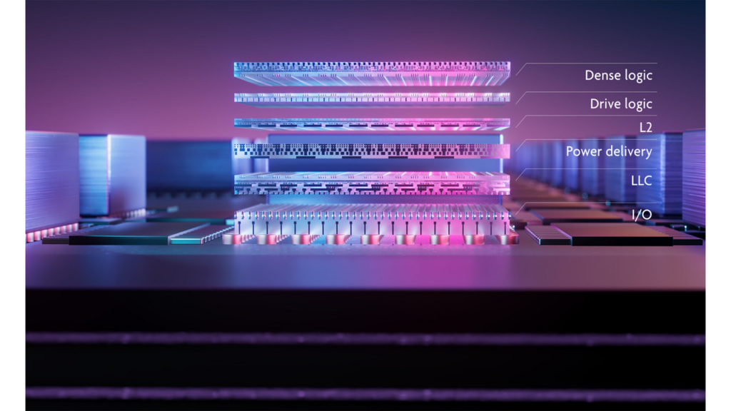
Imec and EV Group Set New World Record for 3D Chip Stacking Precision with Sub-40nm Wafer Bond Overlay
PR Newswire ベルギー Overview Imec and EV Group have achieved a world-record post-bond overlay accuracy of less than 40 nanometers across a 300mm wafer for 200nm pitch hybrid bonding, a crucial advancement for next-generation 3D ICs. Dem... -
TSMC CoWoS Capacity Becomes Major AI Chip Growth Bottleneck: Ramping to 120K Wafers/Month by late 2026 Still Falls Short of Demand
backplane Taiwan Overview TSMC's CoWoS packaging capacity is identified as the most critical bottleneck hindering AI chip evolution. While TSMC plans to quadruple its CoWoS production capacity from approximately 35,000 wafers/month in la... -
KLA’s Advanced Packaging Business Soars, Projecting Over $1.3B Revenue in FY2026 Driven by AI Inspection Demand
Bitget USA Overview KLA Corporation, a global leader in semiconductor process control and yield management, is experiencing rapid growth in its advanced packaging business, driven by the increasing complexity of AI chips. Revenue from th... -
ASMPT Establishes Advanced Packaging Technology Advisory Council to Accelerate AI-Era Innovation
ASMPT Singapore Overview ASMPT has established an Advanced Packaging Technology Advisory Council (TAC) to address the growing importance of advanced packaging for next-generation computing and AI components. The TAC will focus on a broad... -
Aurobindo Pharma Inaugurates ₹10 Billion (USD 120M) TheraNym Biologics CDMO Plant in India, Expanding Capacity by 25,000L
Sahi India Overview Aurobindo Pharma announced the inauguration of its state-of-the-art ₹10 billion (approx. USD 120 million) TheraNym biologics CDMO facility in Hyderabad, India. This plant adds 25,000 liters of mammalian cell culture c...