Semiconductor Back-End– category –
-

Applied Materials Fortifies AI Advanced Packaging with 10-Year TSMC Pact and NEXX Acquisition
Simply Wall St News USA Overview Applied Materials significantly expanded its presence in AI advanced packaging by securing a 10-year strategic partnership with TSMC for AI-focused packaging and completing the acquisition of NEXX. These ... -
Samsung Electronics Advances “2.xD” Packaging Integrating HBM, Logic, and Optical Tech to Resolve AI Power and Heat Bottlenecks
BigGo Finance South Korea Overview Samsung Electronics is developing "2.xD" next-generation packaging technology that integrates High Bandwidth Memory (HBM), logic chips, and silicon photonics (SiPh) into a single package to address crit... -
Malaysia Launches RM92 Million Government-Backed Initiative to Develop HBM4 Advanced Packaging Pilot Line, Targeting Higher Semiconductor Value Chain
Business News Malaysia Overview Malaysia is aggressively pursuing a strategy to elevate its position in the semiconductor value chain by focusing on IC design and advanced packaging. The Malaysia Advanced Packaging Consortium (MAPC), est... -
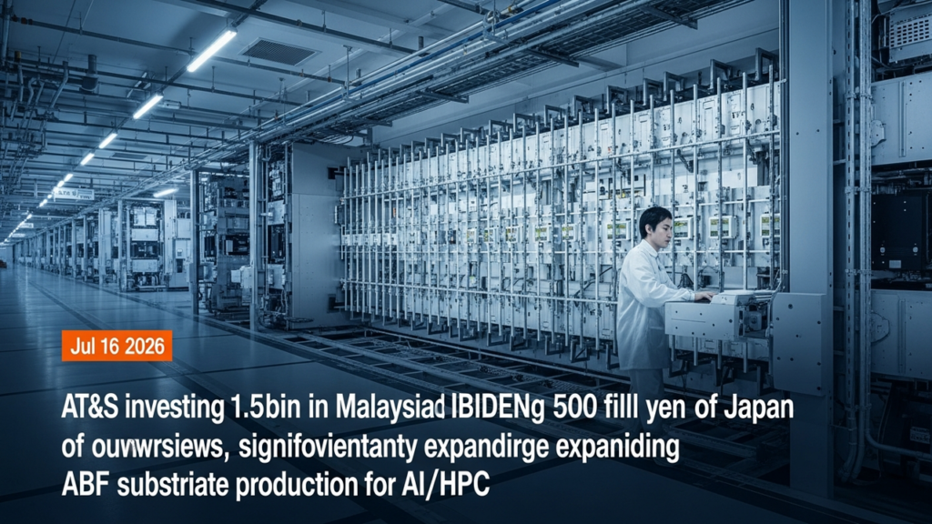
AT&S to Invest €1.5-2 Billion in Malaysian ABF Capacity, While IBIDEN Allocates ¥500 Billion for AI/HPC Substrate Expansion in Japan & Overseas
Sector Signals China Overview AT&S has agreed with AMD and another major tech firm to expand high-end IC substrate capacity for AI/HPC, planning a €1.5-2 billion investment in its Kulim, Malaysia plant, fully supported by long-term c... -
Taiwan’s TGV Glass Substrate Supply Chain Advances: E&R Engineering Ships Laser Modification Equipment to US Client, Accelerating Mass Production
Taiwan News Taiwan Overview Driven by escalating HPC demand, glass substrates are emerging as a next-generation advanced packaging solution, leading to the formation of a robust Through-Glass Via (TGV) supply chain in Taiwan. E&R Eng... -
CoWoS Identified as Core Bottleneck for AI GPU Shipments, Distinct from HBM Shortage
BiyaPay Blog International Overview CoWoS (Chip-on-Wafer-on-Substrate) is an advanced packaging technology integrating GPUs, HBM, and chiplets; its limited capacity forms a critical manufacturing integration bottleneck for AI GPU shipmen... -
NVIDIA’s AI Chip Supply Bottleneck Stems from TSMC’s Booked CoWoS Capacity, Intel EMIB Emerges as Alternative
BingX International Overview TSMC's CoWoS (Chip-on-Wafer-on-Substrate) advanced packaging capacity is fully booked through 2026, with 52-78 week lead times, posing a severe supply bottleneck for NVIDIA. While NVIDIA reportedly secures 60... -
NVIDIA’s 2027 CoWoS Supply Forecast Raised 69% to 1.1 Million Interposers; AMD to See Over 50% Growth: KeyBanc Asia Supply Chain Checks Reveal Strong Demand
TipRanks USA Overview KeyBanc analyst John Vinh's Asia supply chain checks reveal strong, persistent demand across the semiconductor ecosystem. NVIDIA's 2027 CoWoS supply forecast for Rubin and Rubin Ultra was raised 69% to 1.1 million i... -
TSMC and NVIDIA’s ‘Glass Killer’: How Glass Core Substrates Will Revolutionize AI Chips by 2028
SETN Taiwan Overview Renowned analyst Kuo Ming-Chi reveals TSMC's secretive development of 'glass core substrates' in collaboration with NVIDIA, poised to be a game-changer for next-generation AI chip manufacturing. This innovative techn... -
Rapidus and Cadence Partner on Agentic AI for Advanced SoC Design, Driving System-Level Co-Optimization
Las Vegas Sun USA Overview Japan's Rapidus announced a partnership with Cadence to drive system-level co-optimization for Agentic AI-enabled advanced SoC (System-on-Chip) design. This collaboration emphasizes tight integration across sem...