Background: ALD’s Ascendance in Advanced Semiconductor Manufacturing
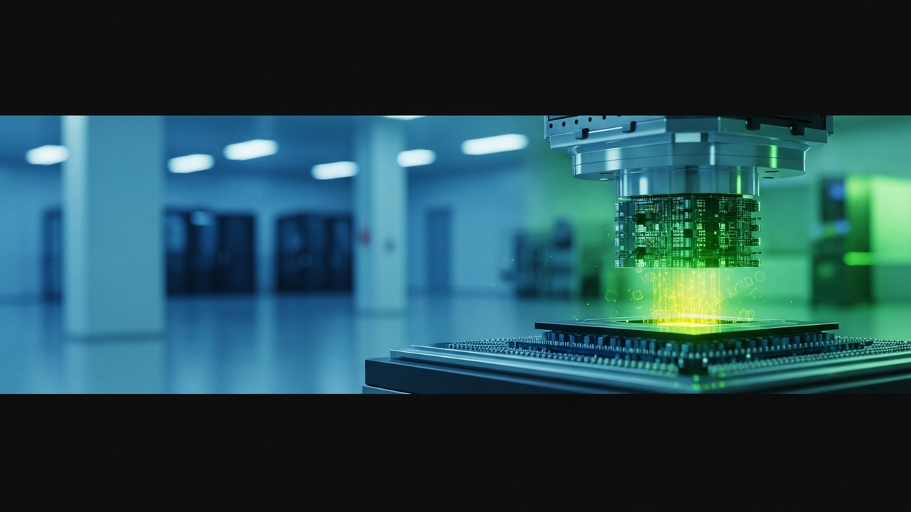
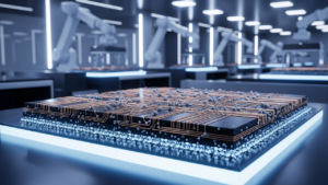
As the semiconductor industry pushes towards sub-2nm process nodes, Atomic Layer Deposition (ALD) has emerged as an indispensable technology for achieving atomic-scale precision in material deposition. The first quarter of 2026 marks a significant “supercycle” for ALD, driven by the escalating demand for 2nm logic nodes and specialized hardware for artificial intelligence (AI). These advanced computing requirements necessitate ultrathin, highly conformal, and defect-free films, conditions ideally met by ALD’s layer-by-layer growth mechanism.
Key Findings / Results: Innovations Driving Performance and Density
Applied Materials has unveiled its pioneering Spectral™ ALD system, engineered to selectively deposit molybdenum as a replacement for tungsten in transistor contacts. This innovation has achieved a remarkable 15% reduction in contact resistance, a critical metric for enhancing the performance and energy efficiency of next-generation AI chips. Such a reduction directly translates to faster switching speeds and lower power consumption, vital for high-density computing. Concurrently, researchers at UC Berkeley have made a groundbreaking discovery: by reducing the thickness of common titanium dioxide (TiO2) to less than 3 nanometers using ALD, they successfully transformed it into a ferroelectric material. This discovery is pivotal for developing ultra-dense, low-power non-volatile memory that is fully compatible with existing silicon manufacturing processes, offering a path towards significantly more compact and efficient data storage solutions. Furthermore, AI is being integrated into ALD reactor designs, optimizing process parameters and accelerating the discovery of new material recipes from conventional timelines of months down to mere weeks. The commercialization of Area-Selective ALD (AS-ALD) represents another significant leap, enabling the precise deposition of atoms only onto specific surface areas, thereby eliminating the need for complex etching steps and facilitating bottom-up nanofabrication. Beyond semiconductors, these ALD advancements are also extending to novel applications such as “atomic armor” for advanced battery technologies, demonstrating the versatility of atomic-scale engineering.
Technical Significance & Outlook: Beyond Moore’s Law
The technical significance of these ALD advancements cannot be overstated. The 15% reduction in contact resistance achieved by Applied Materials is a direct enabler for scaling logic devices beyond the conventional limits of Moore’s Law, allowing for higher transistor density and improved device performance in AI accelerators and high-performance computing. The ferroelectric TiO2 discovery opens an entirely new materials pathway for non-volatile memory, potentially leading to energy-efficient, high-density storage solutions that are crucial for edge AI and IoT devices. The integration of AI into ALD processes represents a paradigm shift in materials discovery and process optimization, significantly reducing R&D cycles and accelerating time-to-market for new semiconductor devices. AS-ALD promises to simplify complex fabrication flows, lower manufacturing costs, and enable novel 3D device architectures. Collectively, these innovations position ALD as a cornerstone technology for the post-CMOS era, not only in advancing semiconductor scaling and performance but also in enabling new functionalities across diverse fields like energy storage, advanced sensors, and quantum computing, solidifying its role as a key driver of 21st-century technological progress.
Source: https://www.atomiclayerdeposition.com/news/posts/what-is-new-in-ald-q1-2026


Comments