Key Findings
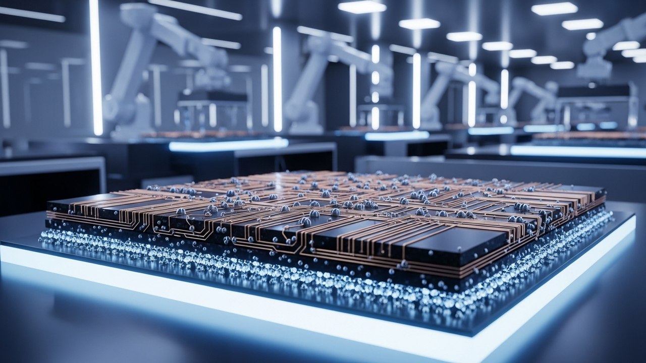
A long-standing challenge in advanced packaging—dielectric loss under high-frequency and high-temperature conditions in existing dielectric materials like epoxy resins—has been resolved with the introduction of a new build-up dielectric material. This breakthrough material demonstrates remarkable performance, reducing signal transmission loss by approximately 40% while maintaining high compatibility with current manufacturing processes. It achieves both ultra-low loss characteristics and robust reliability, which is expected to significantly enhance the performance, reliability, and functionality of integrated circuit (IC) substrates in high-performance computing, telecommunications, and evolving automotive applications.
Technical / Clinical Details
The newly developed build-up dielectric material minimizes signal attenuation in high-frequency ranges, such as millimeter-wave and terahertz bands, by optimizing its dielectric properties at a molecular level. Conventional epoxy resins often suffer from increased dielectric loss tangent (tan δ) beyond certain temperature and frequency ranges, leading to signal degradation and heat generation. The new material successfully achieves a substantial reduction in this dielectric loss tangent, contributing to stable IC operation, particularly in environments demanding high-speed and high-capacity data communication. Furthermore, this material possesses excellent mechanical strength and thermal resistance, ensuring compatibility with standard semiconductor manufacturing processes like photolithography and etching. This compatibility eliminates the need for significant process modifications, facilitating rapid adoption and cost-efficiency.
Background & Context
The proliferation of next-generation technologies such as 5G/6G communication, Artificial Intelligence (AI), High-Performance Computing (HPC), and autonomous driving imposes unprecedented demands on semiconductor chip processing power and interconnect speed. Packaging technology, critical not only for connecting chips to external systems but also for high-density integration while maintaining signal integrity, has often been a bottleneck for overall system performance. Dielectric materials are crucial components in forming signal transmission pathways, and improving their loss characteristics directly translates to enhanced power efficiency and accelerated signal speeds. This technological innovation addresses this bottleneck, pushing the performance limits of next-generation electronic devices.
Strategic Significance & Outlook
The commercialization of this ultra-low loss build-up dielectric material is set to profoundly impact the advanced packaging market, driving accelerated adoption in areas such as high-speed communication infrastructure, data centers, and automotive radar systems. The 40% reduction in signal transmission loss directly translates to lower power consumption and improved operational reliability for devices, ultimately contributing to the realization of smaller, more functional electronic devices. Moving forward, this technology is expected to be further integrated into increasingly miniaturized semiconductor manufacturing processes, serving as a foundational technology for the evolution of future electronics. This will likely further accelerate the adoption of AI and IoT devices, fostering a broader digital transformation across society.
Source: #
Get our weekly technology intelligence — free
Receive an infographic that lets you judge at a glance whether each field’s analysis report is worth reading.
Subscribe Free — Weekly Tech Intelligence
By subscribing, you’ll receive Troy-Technical’s weekly technology intelligence newsletter.
- Your email and selected fields are used only to deliver the newsletter.
- We never share your information with third parties.
- You can unsubscribe anytime via the link in each email.
See our Privacy Policy for details.
Takes about a minute · Unsubscribe anytime







Comments