May 2026– date –
-

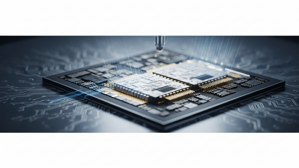
Heterogeneous Integration Advances with Hybrid Bonding, Tackling Critical Power and Thermal Challenges for AI and 5G/6G
IndexBox Global Overview Heterogeneous integration, particularly vertical chip stacking with fine-pitch interconnects, is crucial for future AI and 5G/6G electronics, dramatically reducing data travel distances and power consumption. Hyb... -
Tokyo Electron and Samsung Boost Capex for Hybrid Bonding Equipment Amid Advanced Packaging Shift
Mordor Intelligence Japan, South Korea Overview Tokyo Electron and Samsung are significantly increasing capital expenditures for hybrid bonding and general bonding equipment, targeting long-term growth in the Through-Silicon Via (TSV) ma... -
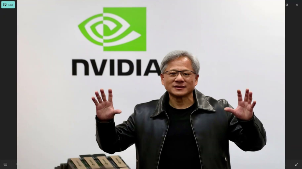
NVIDIA CEO Jensen Huang Projects $150 Billion Annual Investment in Taiwan’s AI Supply Chain
BigGo Finance Taiwan Overview NVIDIA CEO Jensen Huang announced that the company's annual procurement and investment in Taiwan's AI supply chain is projected to reach $150 billion in the future, a tenfold increase from $10-$15 billion fo... -
NVIDIA’s CoWoS Bottleneck Eases, HBM Supply Emerges as Primary Constraint for AI Accelerators
24/7 Wall St. USA Overview TSMC's CoWoS advanced packaging capacity for AI accelerators is expanding, projected to reach 35,000 wafers/month by late 2026 and up to 140,000 wafers/month by 2027, alleviating a long-standing bottleneck. How... -
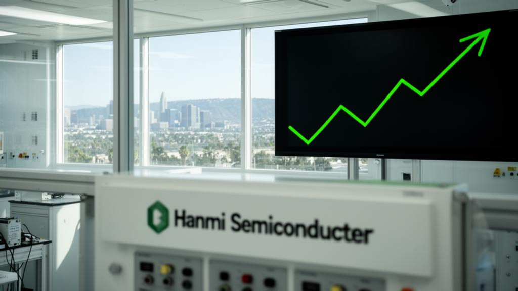
Hanmi Semiconductor Forecasts HBM4 TC Bonder Rebound in Q2, Announces US Expansion Plans
BigGo Finance South Korea Overview Hanmi Semiconductor anticipates a significant rebound in HBM4 TC bonder orders from Q2 2026, driven by accelerating AI semiconductor demand, despite a Q1 slump during the HBM3E-to-HBM4 transition. The c... -
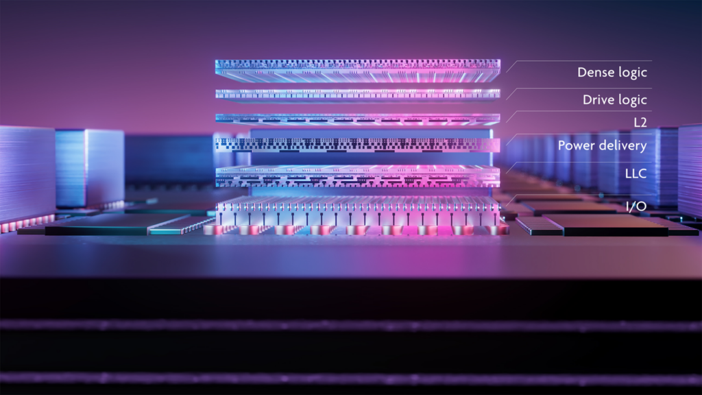
Pushing the Limits of 3D Integration: Imec and EVG Achieve Record 200nm Hybrid Bonding Pitch
imec ベルギー Overview Imec and EV Group (EVG) have announced a major breakthrough in 3D integration, demonstrating wafer-to-wafer hybrid bonding with an unprecedented 200nm copper interconnect pad pitch on 300mm wafers. Achieved with a ... -
ASE Unveils Industry-First Automated 310mm Panel-Level Packaging Line for AI and Chiplet Integration
AnySilicon Taiwan Overview Advanced Semiconductor Engineering (ASE) has developed an automated 310mm x 310mm panel-level packaging (PLP) production line, a significant advancement for AI processors and chiplet architectures. This industr... -
Malaysia Launches National Consortium to Accelerate Advanced Semiconductor Packaging Development Within Two Years
SME.asia Malaysia Overview Malaysia has established the Malaysia Advanced Packaging Consortium (MAPC) with a total funding of RM185 million ($39 million USD) to develop domestic advanced semiconductor packaging capabilities within two ye... -
SK Hynix and Samsung Unveil Production-Ready HBM4 with Hybrid Bonding, Targeting H2 2026 Mass Production
Techfund South Korea Overview At CES 2026, SK Hynix showcased a 16-layer, 48GB HBM4 device leveraging advanced Through-Silicon Via (TSV) and hybrid bonding for high density, while Samsung presented a 12-layer, 36GB HBM4 stack focused on ... -
AMD Commits Over $10 Billion to Taiwan’s AI Ecosystem for Advanced Packaging and EFB Technology Expansion
EE Times Taiwan Overview AMD announced an investment exceeding $10 billion into Taiwan's AI ecosystem, bolstering advanced packaging capabilities and R&D. This initiative specifically targets Elevated Fanout Bridge (EFB) based 2.5D p...