New Technology– category –
-

Tokyo Institute of Science Achieves Sub-Millisecond AI for Semiconductor Inverse Problems
東京科学大学 Japan Overview Scientists at the Tokyo Institute of Science have developed a tandem neural network that solves complex semiconductor inverse problems in under one millisecond. This AI system infers critical material paramete... -
ASCEND Project Launched in Berlin with €30 Million Funding to Revolutionize Catalyst Discovery via AI-Driven Closed-Loop Systems
EurekAlert! Germany Overview The ASCEND project, launched in Berlin with €30 million in funding, aims to usher in a new era of catalyst discovery. This project moves away from traditional trial-and-error by integrating AI models, high-th... -
Kyushu University Pioneers Explainable AI and ChatGPT-Powered ‘Human-in-the-Loop’ for Rapid AEM Material Discovery
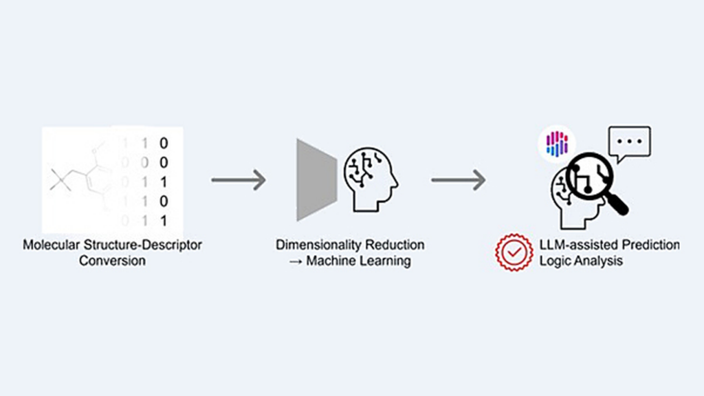
九州大学ニュース Japan Overview Researchers at Kyushu University have developed a novel 'Human-in-the-Loop' framework that efficiently synthesizes explainable AI, ChatGPT, and expert human knowledge to accelerate the development of anion... -
MDPI Paper Develops Machine-Learned MTPs for Low-Cost, High-Accuracy Prediction of Heat Transport in AlGaN and Related Materials
MDPI Switzerland Overview A study published in MDPI reports the development of Machine-Learned Moment Tensor Potentials (MTPs) for simulating static and dynamic structural properties and heat transport in AlGaN and related materials. Tra... -
ResearchGate Paper: Unconstrained MLIPs Achieve Superior Accuracy and Speed with Large Datasets, Enhancing Static Simulations
ResearchGate (Machine Learning: Science and Technology) Unknown Overview A paper published via ResearchGate demonstrates that unconstrained Machine Learning Interatomic Potentials (MLIPs), when trained on sufficiently large datasets, can... -
SandboxAQ Secures $500M from US Department of Commerce Under CHIPS Act to Resolve Semiconductor Materials Supply Chain Challenges
Semiecosystem USA Overview SandboxAQ, an AI-driven materials discovery platform, has received $500 million in government funding from the U.S. Department of Commerce under the CHIPS and Science Act. This funding will enable the company t... -
Radical AI’s Self-Driving Lab Generates 1,200 Alloys in Six Months, Accelerating Materials Discovery
Latent.Space USA Overview Joseph Krause of Radical AI asserts that 'self-driving labs' are indispensable for materials discovery, surpassing the limitations of 'one-shot' AI. His company's autonomous lab, utilizing a closed-loop system c... -
RSC Paper Proposes ‘Digital Materials Ecosystem’ for Autonomous Discovery, Integrating Databases and AI Agents
RSC Publishing UK Overview A paper from RSC Publishing proposes a 'Digital Materials Ecosystem,' a new materials research paradigm integrating data, theory, and automation. This ecosystem combines reliable material databases, physical fr... -
Hugging Face Showcases LLM Application Preprints in Scientific Discovery, Emphasizing Autonomous Agents in Materials, Biology, and Chemistry
Hugging Face USA Overview Hugging Face's Daily Papers featured several arXiv preprints on the application of Large Language Models (LLMs) in scientific discovery. These papers focus on benchmarking LLMs across biology, chemistry, materia... -
Jeff Bezos Backs AI Materials Science Startup CuspAI with $400M Investment, Valuing Company at $2.6B to Accelerate Carbon Capture and Semiconductor Material Development
TechCrunch UK Overview Jeff Bezos has led a $400 million funding round for UK-based AI materials science startup CuspAI, valuing the company at an estimated $2.6 billion. CuspAI aims to dramatically accelerate materials discovery from ye...