Semiconductor Back-End– category –
-

IDTechEx Analyzes New 2.5D/3D Semiconductor Packaging Trends: Glass Interposers and Hybrid Bonding Drive Evolution
IDTechEx UK Overview IDTechEx's analysis highlights glass interposers and hybrid bonding as critical emerging trends in semiconductor packaging. Glass interposers offer compatibility with panel-level packaging, promising cost-effective, ... -
Bonafide Research: Global 3D/2.5D IC Packaging Market Accelerates with UCIe Standard, Forecasts Growth Through 2031
Bonafide Research India Overview This article provides an overview of a market research report published by Bonafide Research. According to Bonafide Research's latest report, the global 3D IC and 2.5D IC packaging market is projected to ... -
HBM Supply Crisis of 2026 Projected to Persist Until 2027, Redefining AI Hardware Deployment Bottleneck
EnkiAI USA Overview Explosive growth in the AI sector has triggered a structural HBM supply crisis, making it the primary bottleneck for AI hardware deployment throughout 2026, projected to last until at least 2027. The market has shifte... -
2026 Chip Crisis Sounds Hardware Wake-Up Call: AI Demand Reshaping Semiconductor Supply Chains
Trax Technologies USA Overview The 2026 chip crisis highlighted modern supply chains' deep reliance on semiconductor availability, where chip access dictates the viability and growth of AI accelerators, warehouse robots, autonomous vehic... -
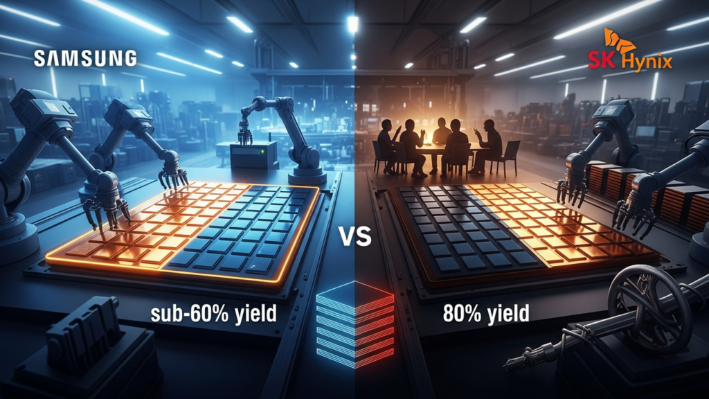
Samsung HBM4 Yield Dramatically Improves from Under 60% to 80%; SK Hynix Labor Talks Stall, Intensifying AI Memory Race
TrendForce Taiwan Overview Samsung's HBM4 yield has dramatically improved from under 60% at launch to 80% within months, according to Seoul Economic Daily. This swift process enhancement by Samsung comes amid tight HBM supply, surpassing... -
AI Accelerates Shift to Panel Level Packaging (PLP) and Glass Core Substrates, Positioning Them as Pillars of Next-Gen Packaging
IEEE / Presentation USA Overview Driven by soaring demand from AI, automotive electronics, and consumer devices, advanced packaging is a critical enabler for enhanced performance, higher integration, and miniaturization in semiconductors... -
SK Hynix Poised to Dominate HBM4 Market with 70% Price Hike and $7B Global Investment for AI Acceleration
SK Hynix South Korea Overview SK Hynix, commanding over 60% of the high-bandwidth memory (HBM) market, projects a nearly 70% price increase for its next-generation HBM4, slated for 2026. To meet soaring AI demand, the company is committi... -
APC 2026: Advanced Packaging, Interconnects, and Chiplets Propel AI Systems Beyond Traditional Scaling
SEMI Europe Europe Overview The Advanced Packaging Conference (APC) 2026 convened to address the critical role of power delivery and interconnect innovations in driving AI system performance. As traditional device scaling approaches its ... -
ECTC 2026 Highlights Advanced Packaging Future: Glass Substrates and FOPLP at the Core of System Innovation
Advanced Packaging Magazine USA Overview ECTC 2026 emphasized a structural shift in semiconductor innovation, moving beyond transistor scaling to packaging and integration technologies. Noteworthy advancements in heterogeneous integratio... -
Samsung’s Aggressive HBM4 Investment Targets Top HBM Market Share Next Year, Attracting NVIDIA and AMD Interest
Sammy Fans South Korea Overview According to UBS forecasts, Samsung Electronics is poised to become the world's leading HBM memory manufacturer next year, driven by aggressive investments and expanded production in HBM4. The rapid surge ...