Semiconductor Back-End– category –
-

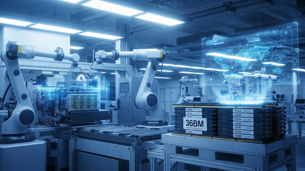
Micron Initiates Mass Production of 36GB 12-Layer HBM4 for NVIDIA Vera Rubin, Boosts US Semiconductor Investment Over $250 Billion
openPR.com USA Overview Micron Technology commenced mass production of its advanced 36GB 12-layer HBM4 memory in March 2026, shipping to NVIDIA for its Vera Rubin platform. This move underscores the market's rapid shift towards higher-ca... -
TSMC Achieves 98-99% Yield for AI Products on CoWoS 5.5x Process, Targets 14x Reticle Size Expansion by 2029
Wccftech Taiwan Overview TSMC Vice President Ho Chun announced remarkable 98% to 99% yields for multiple AI-related products assembled using the CoWoS 5.5x process. This exceptional achievement highlights TSMC's manufacturing prowess in ... -
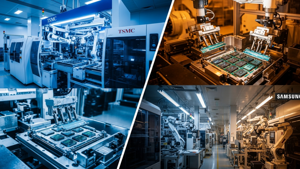
TSMC Doubles Advanced Packaging Capacity Over Three Years; Samsung Expands 2nm & Advanced Packaging Collaboration with Broadcom
BigGo Finance Taiwan Overview TSMC revealed it has doubled its advanced packaging capacity annually for the past three years but still lags behind surging AI chip demand, operating 10 dedicated facilities globally. Meanwhile, Samsung Ele... -
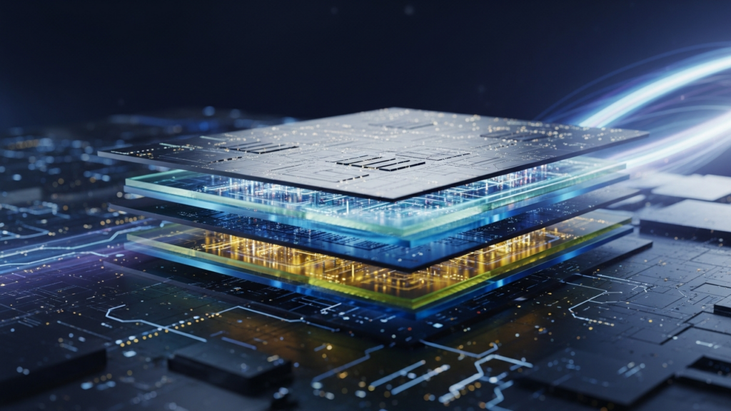
Samsung Unveils zHBM, a 3D Logic-Memory Integrated AI Architecture, Alongside HBM4E/HBM5 Roadmap at FMS 2026
Samsung Semiconductor South Korea Overview Samsung presented its vision for next-generation AI infrastructure at FMS 2026, unveiling its HBM roadmap, including HBM4E and HBM5, and a novel 3D memory architecture called zHBM. This zHBM sol... -
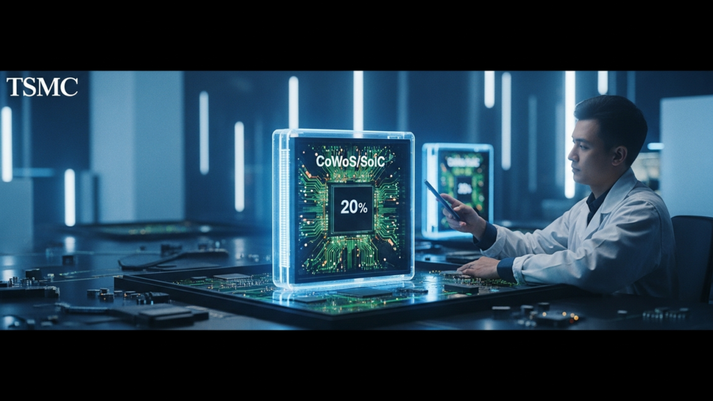
TSMC CoWoS & SoIC Packaging Become Primary AI Chip Bottleneck, Forecasting 10-20% Global Supply Shortfall by 2027 Amidst Doubling Demand
Exponential Industry Taiwan Overview TSMC's CoWoS and SoIC packaging technologies are identified as the primary physical constraints in AI GPU and accelerator production. Global CoWoS demand is projected to double from 1.3-1.4 million wa... -
JEDEC Relaxes HBM4 Package Height to 775 µm, Enabling 12-Hi/16-Hi Stacks Without Immediate Cu-Cu Hybrid Bonding
Exponential Industry USA Overview JEDEC has relaxed the HBM4 package height specification from 720 µm to 775 µm, allowing for 12-Hi and 16-Hi stack HBM modules without immediate reliance on Cu-Cu hybrid bonding. HBM utilizes 3D stacked D... -
Applied Materials Reports $9.12 Billion in Q3 2026 Revenue, Plans to Double Semiconductor Systems Output by 2028 Amid Surging Demand
GlobeNewswire USA Overview Applied Materials announced Q3 2026 revenue of $9.12 billion, marking a 25% year-over-year increase and slightly exceeding market expectations. The company maintains strong leadership and a pipeline of innovati... -
KLA Forecasts $1.1 Billion in Advanced Packaging Revenue for 2026, Driven by Surging AI and HBM Demand
Quartz USA Overview KLA Corporation anticipates its advanced packaging business revenue will reach approximately $1.1 billion in 2026, representing over 70% year-over-year growth, fueled by increasing AI infrastructure investments and se... -
Ibiden Commits ¥500 Billion to ABF Substrates for AI Servers, Anticipating Supply Crunch Beyond 2028
MK Japan Overview Ibiden, the world's leading AI substrate manufacturer, announced a ¥500 billion investment from this year to 2028 to expand production capacity for IC package substrates for AI and high-performance servers. Despite long... -
AI Demand Strains CoWoS and SoIC Supply: Global Demand to Double to Over 2.5M Wafers by 2027, Facing 10-20% Shortfall
Exponential Industry USA Overview TSMC's CoWoS and SoIC advanced packaging technologies are now the primary physical constraints for AI GPU and accelerator production. Global CoWoS demand is projected to double from 1.3-1.4 million wafer...