Semiconductor Back-End– category –
-

Advanced Semiconductor Packaging & Chiplet Show (ASPS) 2026 in Suwon, Korea, to Cover Advanced Packaging, Chiplets, and HBM
Advanced Semiconductor Packaging & Chiplet Show (ASPS) South Korea Overview The Advanced Semiconductor Packaging & Chiplet Show (ASPS) will take place from August 26-28, 2026, at the Suwon Convention Center in South Korea. This B2B e... -
Glass Substrates Emerge as AI Packaging Game-Changer, Igniting Global Race Towards Mass Production as China and Japan Intensify Competition for Yield Stabilization
The Economy South Korea Overview As AI semiconductor competition shifts from process-node miniaturization to advanced packaging, China and Japan are intensifying efforts to lead the glass core substrate market, a cornerstone for next-gen... -
IMAPS Device Packaging Conference 2026 PDCs Focus on Advanced Packaging for Chiplets and Heterogeneous Integration, Highlighting Hybrid Bonding
IMAPS USA Overview IMAPS Device Packaging Conference 2026 Professional Development Courses (PDCs) extensively covered "Advanced Packaging for Chiplets and Heterogeneous Integration." The courses defined various 2D to 3.5D IC integrations... -
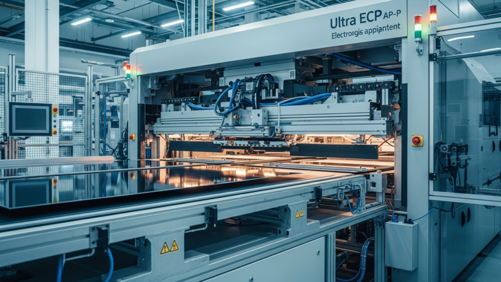
ACM Research Secures Production and Evaluation Orders for Ultra ECP ap-p Horizontal Panel Electroplating Tool, Supporting 600x600mm Panels
GlobeNewswire USA Overview ACM Research announced securing production and evaluation orders from two advanced packaging customers for its Ultra ECP ap-p horizontal panel-level electroplating tool. This innovative tool supports large pane... -
AI’s Performance Breakthrough: Advanced Packaging, Power, and Interconnects Take Center Stage at SEMI Europe 2026
SEMI Europe Europe Overview SEMI Europe's 2026 Advanced Packaging Conference (APC) will spotlight 'Power and Interconnects Innovations Enabling AI System Performance,' emphasizing advanced packaging (AP) and test as crucial for scaling n... -
Semiconductor Back-End Weekly Report August 2, 2026
▼ ▼ ▼ If the infographic makes you want to read the full report, please click the download button below. ▼ ▼ ▼ 📄 Weekly Report August 02, 2026 (PDF) — Download Weekly Report August 02, 2026 (PDF) — DownloadDownload 🎙 Podcast August 02, ... -
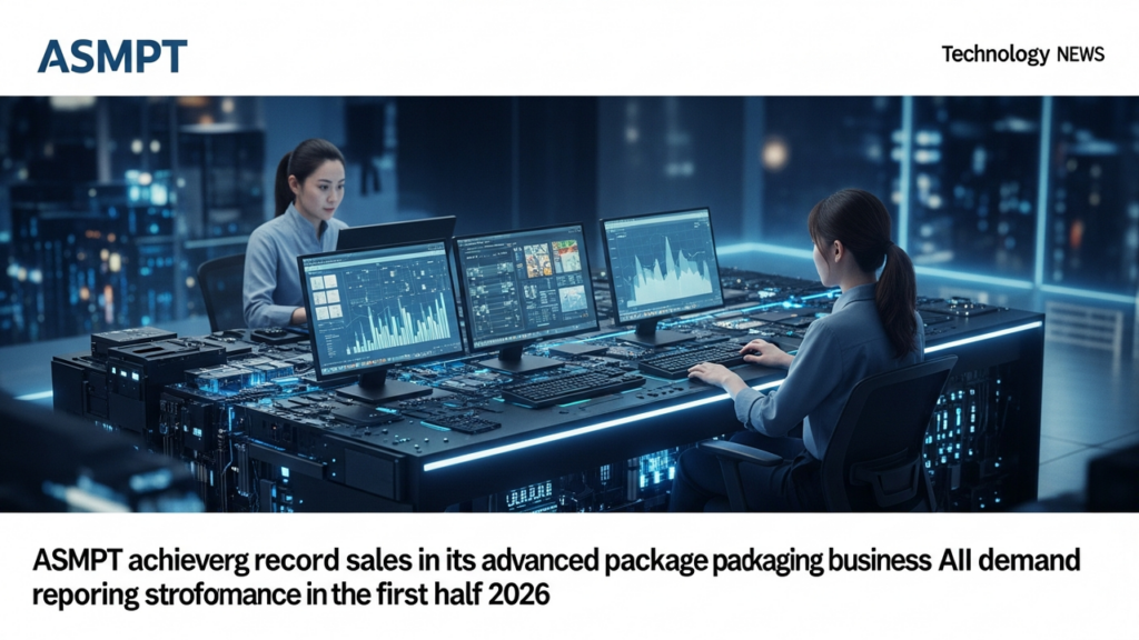
ASMPT’s Advanced Packaging Business Achieves Record Sales in H1 2026, Driven by Surging AI Demand
ASMPT Singapore Overview ASMPT reported robust financial results for the first half of 2026, with its Advanced Packaging (AP) business achieving record sales, significantly propelled by escalating AI demand. Key contributors included The... -
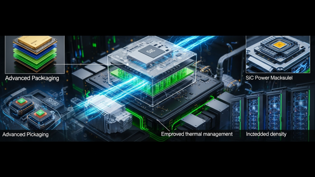
SiC Power Modules Get a Boost: Advanced Packaging with AMB and Embedded Die Transforms EV and AI Data Centers
[Industry Publication/Research] Global Overview Advanced packaging technologies for Silicon Carbide (SiC) power modules are dramatically improving thermal management and power density in electric vehicle (EV) inverters and AI data center... -
ASE Technology Bets Big on AI: $10.5 Billion Record Capex to Double Advanced Packaging by 2027
TrendForce Taiwan Overview ASE Technology Holding is significantly increasing its 2026 capital expenditure to a record $10.5 billion, aiming to double the revenue of its leading-edge advanced packaging (LEAP) business by 2027. This ambit... -
Amkor to Invest $7 Billion in Arizona for Advanced AI Chip Packaging, Shifts Korean SiP Production to Vietnam
Seeking Alpha USA Overview Amkor Technology is making a monumental $7 billion investment to construct an advanced packaging and test campus in Arizona, slated for production by early 2028, to address the escalating demand for AI chips. T...