Semiconductor Back-End– category –
-

Applied Materials Unveils New Systems to Accelerate DRAM and Advanced Packaging for AI Chips
Applied Materials, Inc. USA Overview Applied Materials has introduced a suite of new material engineering systems designed to accelerate the manufacturing of advanced 3D chip architectures crucial for next-generation AI. These innovation... -
Semiconductor Back-End Weekly Report May 20, 2026
▼ ▼ ▼ If you found the infographic compelling and want to read the full Weekly Report, click below to download the Strategy Report. ▼ ▼ ▼ 📄 Semiconductor Back-End Weekly Report — June 20, 2026 Semiconductor_BackEnd_WeeklyReport_EN_20260... -
imec Breaks New Ground: III-V Chiplets on RF Silicon Interposer Achieve 100x Capacitance Density Boost and Sub-600nm Precision
OriginBrief ベルギー Overview imec has announced a significant breakthrough in heterogeneous integration, successfully integrating III-V chiplets onto a 300mm RF silicon interposer platform. This achievement delivers a 10-100x increase i... -
Amkor Technology Shifts SiP Production to Vietnam to Enhance High-Value Programs, Driven by Strong Demand for Advanced Packaging in Premium Smartphones
TradingView USA Overview Amkor Technology continues to benefit from robust demand for advanced packaging solutions like flip-chip and System-in-Package (SiP), fueled by increased semiconductor content in premium smartphones. The company ... -
Nokia Announces Major Expansion of U.S. Advanced Semiconductor Test and Packaging Operations in Pennsylvania, Doubling Workforce to Over 500, to Bolster AI Infrastructure
GlobeNewswire USA Overview Nokia has unveiled a major expansion of its Advanced Test and Packaging (ATP) operations in Allentown, Pennsylvania. This investment aims to enhance domestic production capacity for optical networking technolog... -
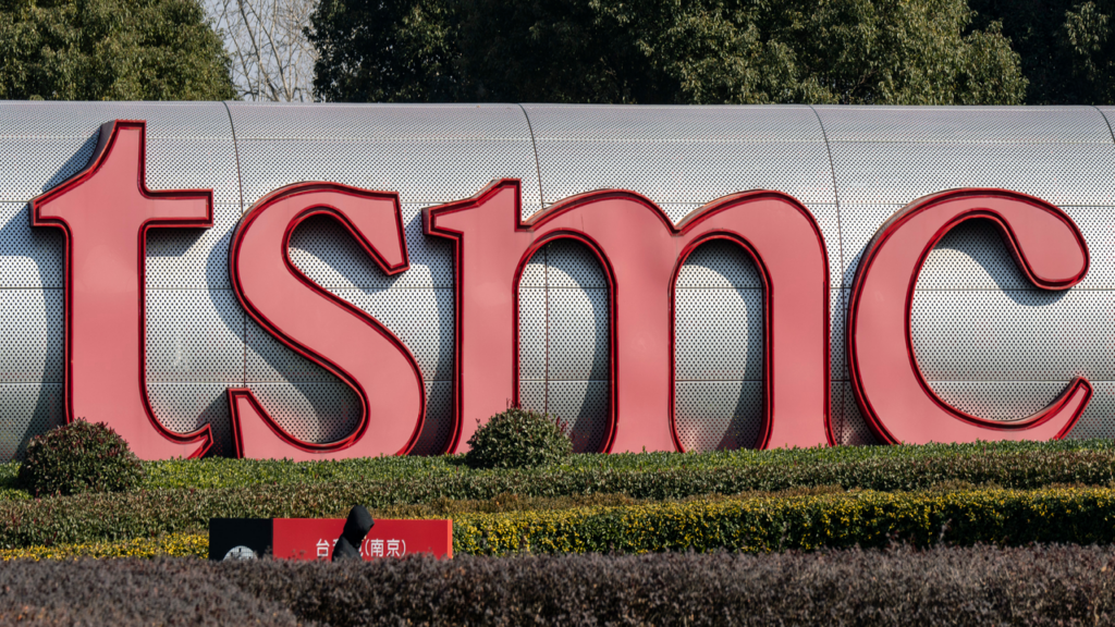
TSMC Accelerates CoPoS Packaging Development, Standardizing 310x310mm Panel Format; Introduces Glass Core Substrate for CoWoS Towards Late 2028 Mass Production
TrendForce Taiwan Overview TSMC is accelerating the development of its CoPoS (Chip-on-Panel-on-Substrate) packaging architecture, standardizing a 310x310mm panel format, with pilot production targeted for 2027 and mass production in late... -
SK hynix Begins Shipping Next-Gen HBM4E AI Memory Chips with 12-Layer Stack, 48GB Capacity, 16Gbps per Pin, and Over 20% Power Efficiency Boost
Bisinfotech South Korea Overview SK hynix has commenced shipments of its next-generation HBM4E AI memory chips, featuring a 12-layer stack with 48GB capacity, ultra-fast data transfer rates of up to 16Gbps per pin, and over 20% improved ... -
Samsung Considers New HBM-Focused Advanced Semiconductor Packaging Plant in South Korea’s Honam Region to Meet AI Server Demand
SamMobile South Korea Overview Samsung Electronics is exploring the construction of a new advanced semiconductor packaging facility in South Korea's Honam region, with Gwangju emerging as a prime candidate. This project aims to bolster S... -
Intel Appoints Former SK hynix CEO Lee Seok-hee as Senior VP of Advanced Packaging to Bolster AI Systems
The Korea Herald South Korea Overview Intel has appointed Lee Seok-hee, former CEO of SK hynix and SK On, as Senior Vice President of Intel Foundry. Lee will lead advanced packaging, system integration, back-end technology development, a... -
Amkor Supercharges U.S. Chip Packaging with 67-Acre Arizona Expansion, Aiming for First High-Volume Advanced OSAT
StocksToTrade USA Overview Amkor Technology has significantly expanded its U.S. presence by acquiring an additional 67 acres at its advanced packaging and test campus in Peoria, Arizona. This strategic move targets establishing the natio...