Key Findings
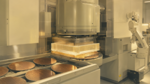
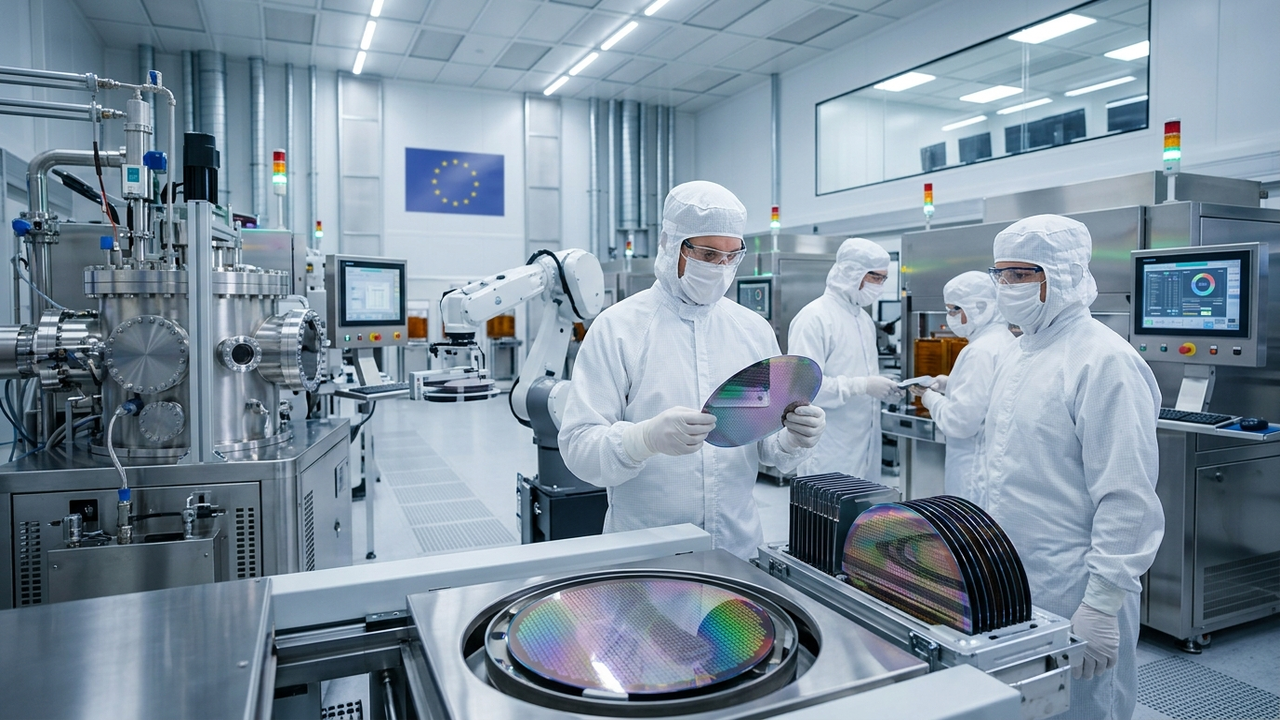
Graphenea has announced the establishment of a new wafer-scale graphene production facility in Europe. This strategic expansion is a groundbreaking step designed to dramatically increase the supply of high-quality graphene, specifically accelerating its commercial applications in the semiconductor and advanced electronic components sectors.
Technical / Clinical Details
The new facility will leverage state-of-the-art Chemical Vapor Deposition (CVD) technology combined with proprietary process optimization to efficiently produce highly uniform, wafer-sized graphene. This approach is projected to reduce manufacturing costs and increase production volume compared to conventional methods. The stable supply of high-quality graphene, compatible with 8-inch and 12-inch silicon wafers, will facilitate its integration into next-generation semiconductor devices, high-speed transistors, transparent conductive films, and high-sensitivity sensors. Specific process improvements are slated to reduce defect density and enhance carrier mobility in CVD graphene, pushing the boundaries of material performance.
Background & Context
Graphene, celebrated as a “wonder material” for its exceptional electrical conductivity, mechanical strength, and transparency, has long faced challenges in achieving large-scale, high-quality production. The semiconductor industry, nearing the physical limits of silicon-based devices, views graphene as a leading candidate for next-generation materials. Graphenea’s announcement represents a crucial milestone in overcoming these production hurdles, signifying graphene’s transition from laboratory-scale research to industrial-scale application. The European Commission has also invested heavily in graphene research, aligning with this strategic facility establishment.
Strategic Significance & Outlook
This new production facility is expected to bolster the European graphene ecosystem and serve as a central hub for driving regional technological innovation. Graphenea plans to leverage this expanded capacity to deepen partnerships with semiconductor manufacturers and electronic device developers, accelerating the market introduction of graphene-based products. This makes the day when graphene provides innovative solutions across computing, telecommunications, and IoT devices more tangible. In the long term, graphene is anticipated to become a new growth driver for the semiconductor industry, fostering the creation of novel products that significantly outperform existing technologies.
Source: #
Get our weekly technology intelligence — free
Receive an infographic that lets you judge at a glance whether each field’s analysis report is worth reading.
Subscribe Free — Weekly Tech Intelligence
By subscribing, you’ll receive Troy-Technical’s weekly technology intelligence newsletter.
- Your email and selected fields are used only to deliver the newsletter.
- We never share your information with third parties.
- You can unsubscribe anytime via the link in each email.
See our Privacy Policy for details.
Takes about a minute · Unsubscribe anytime