Key Findings
Intel’s EMIB-T substrate technology has demonstrated significant advancements, as reported at the ECTC 2026 technology update. This innovative packaging solution has achieved an ultra-fine 25 μm first-level interconnect bump pitch and supports large package dimensions up to 120 × 120 mm. Crucially, it now offers robust support for next-generation memory and interconnect standards, including 12 Gb/s HBM4e and 64 Gb/s UCIe transmission, marking a pivotal step for high-performance chiplet integration.
Technical / Clinical Details
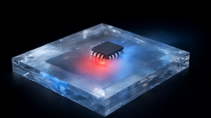
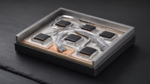
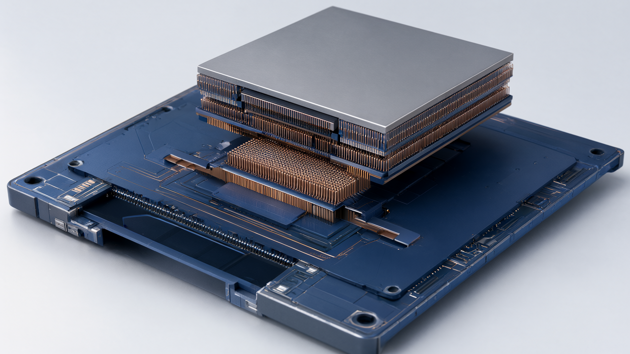
Intel’s EMIB-T (Embedded Multi-die Interconnect Bridge – Thin) substrate technology employs a sophisticated approach where localized silicon bridges, equipped with through-silicon vias (TSVs), are directly embedded within the package substrate. This architecture enables high-density chip-to-chip interconnections. Specific technical breakthroughs reported at ECTC 2026 include:
- First-Level Interconnect Bump Pitch: Achieved a fine pitch of 25 μm. This is fundamental for maximizing data transfer bandwidth between chiplets and enabling extremely high-density connectivity.
- Package Dimensions: Capable of supporting up to 120 × 120 mm packages. This offers enhanced flexibility for integrating multiple large chiplets into a single, cohesive package.
- HBM4e Support: Enables 12 Gb/s High Bandwidth Memory (HBM4e) transmission. This addresses the escalating memory bandwidth requirements of high-performance AI accelerators and High-Performance Computing (HPC) systems.
- UCIe Support: Provides support for 64 Gb/s Universal Chiplet Interconnect Express (UCIe) transmission. This facilitates high-speed, standardized interconnections between chiplets from various vendors, fostering an open chiplet ecosystem.
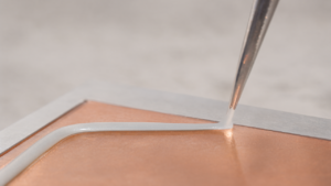
The manufacturing process for EMIB-T involves several complex and critical steps: precise preparation of substrate cavities, accurate placement and bonding of the silicon bridges, meticulous build-up of dielectric and copper layers, and final underfill or bonding operations.
Background & Context
With the relentless advancement of AI and HPC, semiconductor performance scaling is shifting from monolithic die designs to integrating multiple smaller chiplets. In this heterogeneous integration paradigm, packaging technologies that provide fast and efficient inter-chiplet communication are paramount for both performance and cost-effectiveness. Intel’s EMIB technology has been recognized as a cost-effective alternative to traditional interposer-based 2.5D packaging, striking a balance between performance and integration density. EMIB-T further evolves this technology by accommodating next-generation interfaces like HBM and UCIe, aiming to establish new standards for AI-era semiconductor packaging.
Strategic Significance & Outlook
These advancements in Intel’s EMIB-T substrate technology significantly broaden the possibilities for chiplet integration across a wide range of high-performance computing applications, including AI, HPC, data centers, and edge devices. The fine 25 μm bump pitch and support for HBM4e/UCIe will have a profound impact on future semiconductor design and manufacturing. EMIB-T is expected to accelerate the development of semiconductor solutions offering higher performance, greater power efficiency, and enhanced flexibility, thereby driving the further evolution of the chiplet ecosystem. This technology is poised to become a cornerstone in the industry’s overarching heterogeneous integration strategy.
Source: https://www.bestpcbs.com/blog/2026/10/emib-t-substrate/
Get our weekly technology intelligence — free
Receive an infographic that lets you judge at a glance whether each field’s analysis report is worth reading.
Subscribe Free — Weekly Tech Intelligence
By subscribing, you’ll receive Troy-Technical’s weekly technology intelligence newsletter.
- Your email and selected fields are used only to deliver the newsletter.
- We never share your information with third parties.
- You can unsubscribe anytime via the link in each email.
See our Privacy Policy for details.
Takes about a minute · Unsubscribe anytime