TECHNOLOGY EXPLAINER
What Co-Packaged Optics (CPO) Is
— bringing light all the way into the package
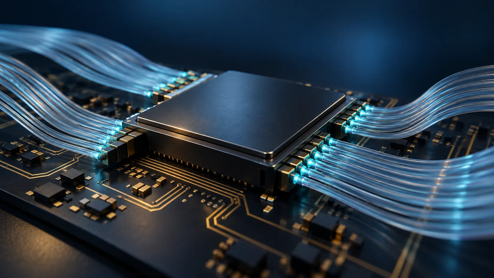
Until now, optical fibre stopped at the front panel of the box. From there to the chip, the signal travelled as electricity. That electrical stretch has become the single biggest source of waste. CPO puts the optical converter inside the same package as the chip. Housing electronics and photonics — two things with nothing physical in common — in one encapsulated body changes what the materials have to do.
- What CPO is (the short version)
- Why it became necessary — the distance to the front panel
- What the numbers actually say
- What is inside the package
- A materials engineer's view 1: why only the laser stays outside
- A materials engineer's view 2: what a light-carrying material must do
- What is still hard
- Glossary / Primary sources / Claim-to-source audit
Sourced = stated in published material from a company or standards body (link given)
Our calculation = a figure this article derived, with the assumptions spelled out
Not yet confirmed = announced plans with no confirmed track record
Structural readings and materials-design interpretation are marked separately as Commentary.
1. What CPO is (the short version)
Co-Packaged Optics means putting the parts that convert electricity into light inside the same package as the processor or switch.
- The old way: the converter is a pluggable optical module in the front panel. Everything from the chip to that module travels as electricity.
- CPO: the converter sits right beside the chip, inside the same package. The electrical run shrinks to a few millimetres.
- Why now: as AI switches grew in capacity, the power and loss of that electrical stretch stopped being negligible.
Resonac calls this class of assembly an optoelectronic fusion package, describing it as one that incorporates conversion between optical and electrical signals, and which is expected to improve data processing capability over today's leading 2.xD packages while also substantially reducing operating powerSourced.
The assembly technologies that make CPO possible are already covered elsewhere in this series.
- Stacking an electrical die on a photonic die (TSMC COUPE) → Heterogeneous Integration
- The platform that links many dies inside one package (CoWoS) → CoWoS and Interposer
- Glass substrates and optical wiring → Glass Substrate
This article deals with the reason anyone goes to this trouble, and with the new material requirements that handling light creates.
2. Why it became necessary — the distance to the front panel
The heart of the problem is surprisingly physical. It is distance.
NVIDIA describes the conventional path this way: "the data signal must traverse long electrical paths from the switch ASIC to the PCB, connectors and finally into the external transceiver before being converted to an optical signal. This segmented journey incurs substantial electrical loss"Sourced.
Broadcom puts the same point as "high power required to equalize signal through PCB and multiple connector discontinuities"Sourced.
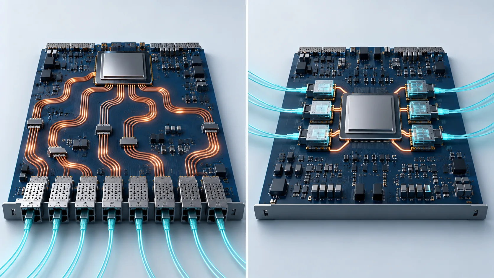
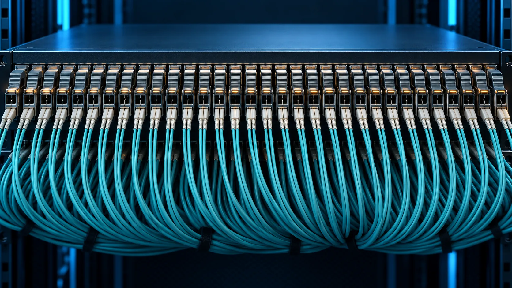
Broadcom sums up the limit of the module approach as "module solutions are still limited by face plate density, MFG costs, and power constraints"Sourced. A front panel is a flat surface with a hard physical limit on how many things fit on it. Switch bandwidth keeps rising; the panel area does not (our commentary).
3. What the numbers actually say
Several companies have published concrete figures for the benefit. Here are three of them.
In its product announcement NVIDIA states that moving to CPO delivers "4x fewer lasers", "3.5x more power efficiency", "63x greater signal integrity", "10x better network resiliency at scale" and "1.3x faster deployment"Sourced. Broadcom reports "30% power savings" for Bailly, and for CPO in general that "CPO provides lower power, architecture scaling to 200G/lane, 50% less components"Sourced.
Every one of these figures was published by a company promoting its own approach. Measurement conditions, comparison baselines and system configurations all differ, and this article has not verified them. They are not general numbers that CPO guarantees (our note).
4. What is inside the package
Broadcom has published the configuration of its CPO switch, Bailly: a 51.2T switch with eight silicon photonic engines (6.4T and 64 channels each) on the same substrateSourced.
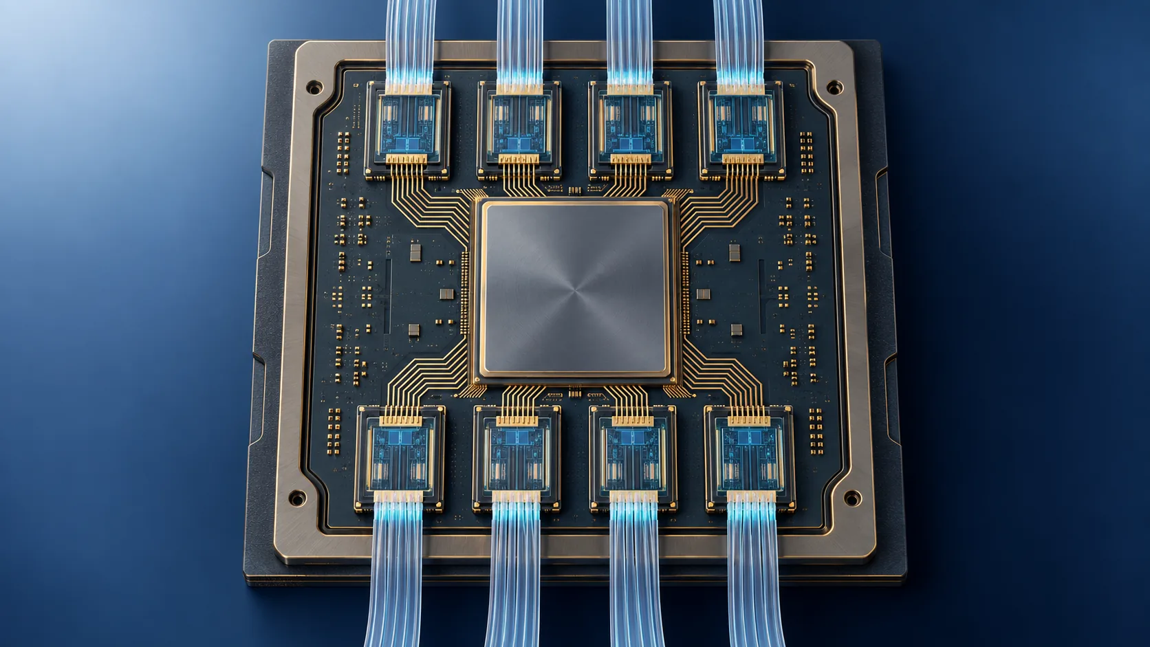
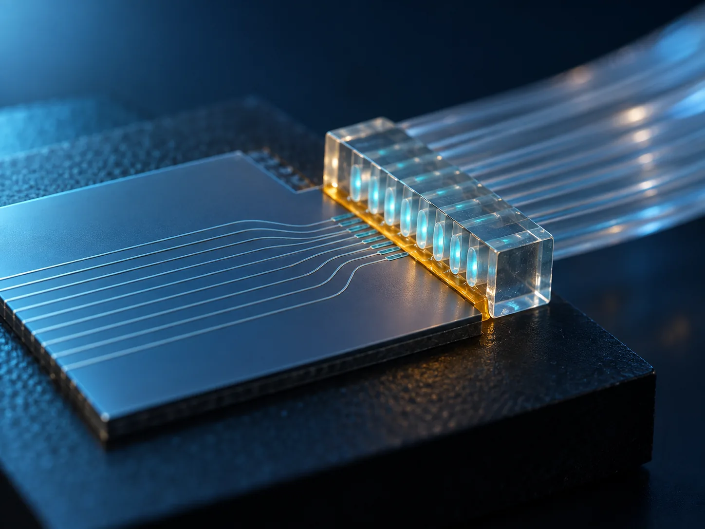
On the NVIDIA side, the construction of the optical engine is described. TSMC's silicon photonics technology COUPE "integrates electronic integrated circuits (EIC) with silicon photonic integrated circuits (PIC) using the 3D chip-on-wafer and chip-stacking packaging technologies"Sourced. In other words, the COUPE covered in the Heterogeneous Integration article is itself a component of CPO.
5. A materials engineer's view 1: why only the laser stays outside
Look carefully at a CPO diagram and something odd appears. For a technology built around light, the light source itself is not in the package.
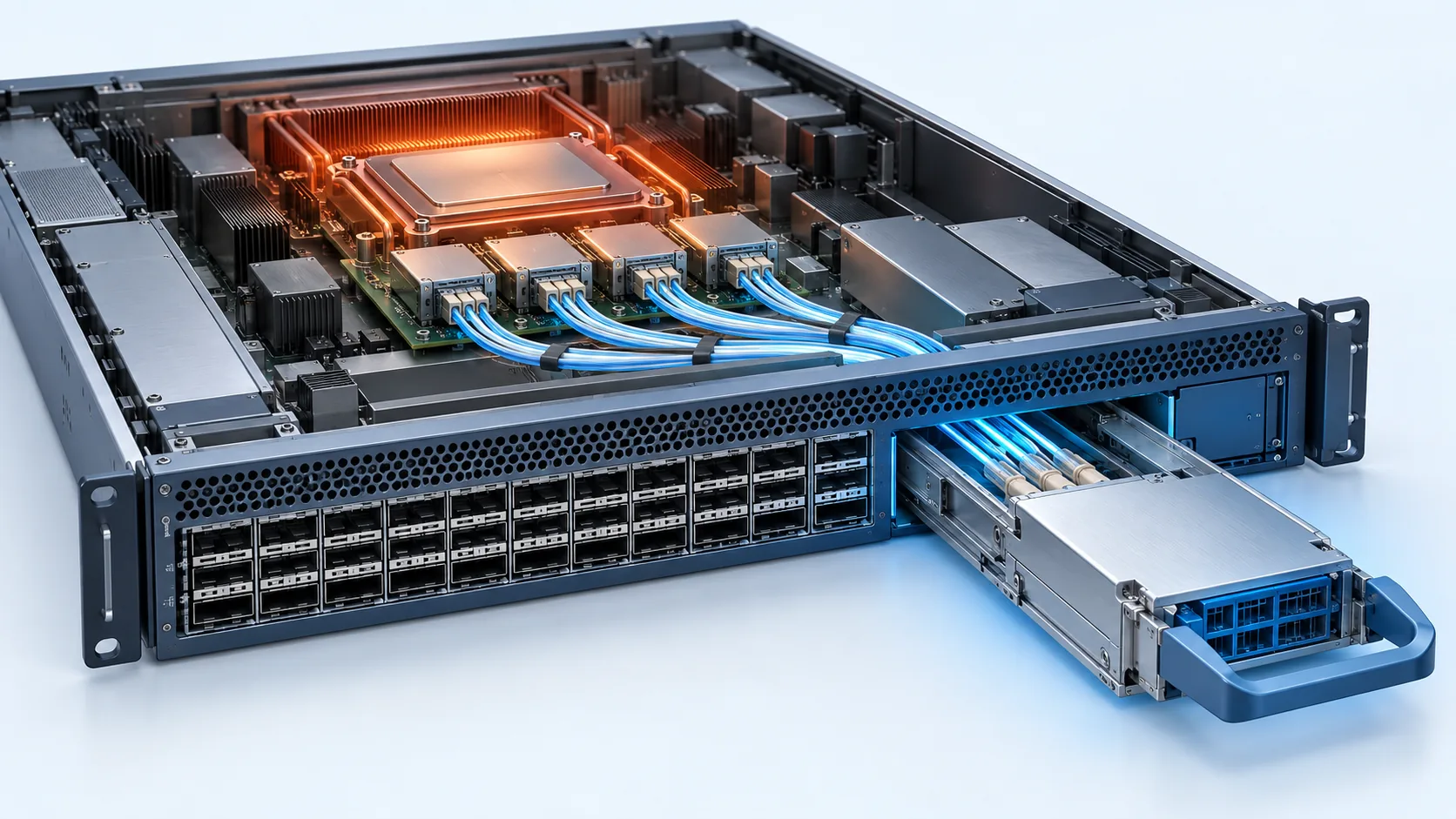
In NVIDIA's arrangement the lasers sit in an ELS (External Laser Source) module in the front panel. The stated reason is "facilitating quick diagnosis and easy replacement while the switch core remains sealed"Sourced.
That placement is now written into an industry standard. On 8 August 2023 the OIF announced the ELSFP (External Laser Small Form-Factor Pluggable) Implementation AgreementSourced. Its purpose is to place the laser source at the front panel, the most cooled section of the system, improving system reliability and enabling efficient hot-swap field replacement when requiredSourced.
Only the laser is treated differently in a CPO design. There are two reasons, and they are worth separating.
- Reliability: OIF chose the most cooled section of the system as the location, and ties that to improved system reliabilitySourced
- Serviceability: OIF cites hot-swap field replacement; NVIDIA cites diagnosis and replacement while the switch core remains sealedSourced
The defining characteristic of CPO is that nothing inside can be unplugged. It gives up the single greatest advantage of pluggable optics: module-level replacement. Which is precisely why the part most likely to fail, and most sensitive to heat, was left somewhere it can still be pulled out.
This is a familiar move in materials engineering. The test socket in the Bonding article changed material from region to region; here, the design changes location from part to part. If heterogeneous integration is about what goes together, CPO is also a deliberate decision about what does not (our commentary).
One more detail: the OIF ELSFP agreement places a multi-fibre blind-mate optical connector at the rear of the module and describes this as reducing eye-safety risk in applications handling high optical powerSourced. Once laser light is present, safety design becomes part of the connector specification itself — a requirement electrical connectors never had (our commentary).
6. A materials engineer's view 2: what a light-carrying material must do
Here is where the genuinely new territory starts for materials suppliers. Light now travels inside the package. Properties that electrical wiring never needed suddenly become requirements.
AGC lists three features for its polymer waveguides (PWG) and glass waveguides (GWG) for optical wiringSourced.
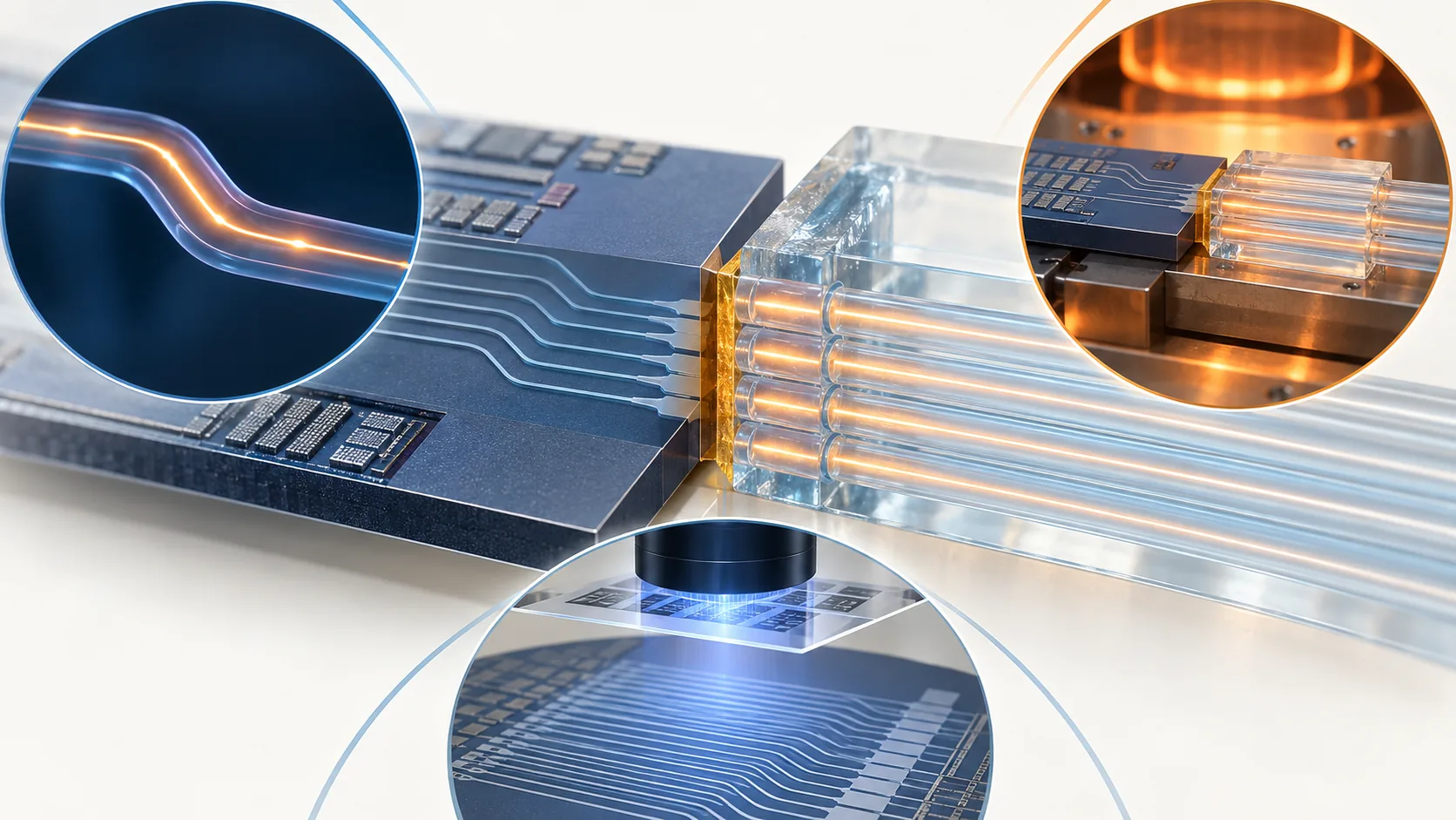
AGC lists high transmittance (O band / C band), reflow compatibility and durability against high-power lasers, and fine patterning by photolithography side by sideSourced. Written as a list they look complementary. To a materials designer they point in different directions.
- Transmittance improves when you remove absorbing structures such as C-H bonds
- Reflow resistance improves with more crosslinking and higher heat resistance — but changing the structure changes the absorption
- Laser durability means not decomposing under continuous illumination. A material that degrades under light gets lossier over time
- Photolithographic patterning requires photosensitivity, which means deliberately adding groups that react to light — the opposite of light stability
The last two are in outright conflict. You want the material to react to light while you build it, and to ignore light while it works. The same tension appears with the photosensitive polyimide and PBO in the RDL article, but here it comes with the extra condition that light travels through the film itself (our commentary).
And one more. The adhesive that joins PIC to FAU, shown by Resonac, is not simply an adhesiveSourced. Light crosses that bond line, so it must be transparent, index-matched, and dimensionally stable over temperature. The adhesive is being asked to perform as an optical component (our commentary).
7. What is still hard
(1) If it fails, the whole package fails
The biggest weakness of CPO, as already noted, is that nothing can be replaced. That also feeds straight back into manufacturing yield.
Bailly puts eight optical engines in one packageSourced. If the yield of a single optical engine is p, the probability that all eight are good is p to the eighth powerOur calculation.
Assumption: a simple calculation treating each engine as independent. In reality redundant channels, pre-screening (KGD) and repair steps change the outcome, so it will not work out this way.
95% each still means only 66% for eight. With pluggable optics you replace one bad module; with CPO, one bad optical engine can mean discarding the switch ASIC with it (our commentary). NVIDIA's statement that CPO involves "fewer components, significantly reducing the likelihood of transceiver failures"Sourced is, among other things, an answer to that worry.
(2) Without standards, it becomes one vendor's technology
Pluggable optics succeeded because the specification was common and any vendor's module fitted the socket. CPO sits inside the package, so left alone it would fragment company by company. That is what the OIF's standardisation work addresses.
(3) The supply chain widens abruptly
In its product announcement NVIDIA names as co-development partners TSMC, Browave, Coherent, Corning, Fabrinet, Foxconn, Lumentum, SENKO, SPIL, Sumitomo Electric and TFC CommunicationSourced.
Semiconductor makers, optical device makers, fibre and connector makers, contract assemblers — this is visibly not the cast of a conventional semiconductor package. Bringing light inside also means bringing the optical communications supply chain inside the semiconductor package (our commentary).

CPO is less a technology for raising performance than a technology for removing waste.
- What it removes: the distance signals travel electrically, the loss along it, and the power spent compensating
- What it gives up: the ability to replace a module in the field
- What it kept: the laser, left somewhere it can still be pulled out (ELSFP)
- What it newly requires: materials that carry light, adhesives that carry light, and connections that do not lose it
For a materials supplier the implication is direct. Materials that used to be judged on conduction, insulation, heat removal and adhesion now gain an extra axis: optical transmission. And that axis often points against the existing ones, as Section 6 showed (our commentary).
8. Glossary
- CPO
- Co-Packaged Optics. Housing the optical conversion parts in the same package as the processor or switch.
- Optoelectronic fusion package
- A package with optical-electrical conversion built in. The term Resonac uses for this class of assembly.
- Pluggable optical module
- An optical transceiver that plugs into the front panel of the equipment. The conventional approach.
- Optical engine
- The integrated component that converts between electricity and light, built in silicon photonics.
- Silicon photonics
- Building optical circuits on silicon, using semiconductor manufacturing equipment.
- PIC
- Photonic Integrated Circuit.
- EIC
- Electronic Integrated Circuit. Combined with a PIC to make an optical engine.
- COUPE
- TSMC's silicon photonics technology, integrating EIC and PIC by 3D stacking (see the Heterogeneous Integration article).
- FAU
- Fiber Array Unit. A part that aligns several optical fibres for connection to a PIC.
- Optical waveguide
- A light path inside a substrate or package. Made of polymer (PWG) or glass (GWG).
- ELS
- External Laser Source. A light source placed outside the optical engine.
- ELSFP
- External Laser Small Form-Factor Pluggable. The standard for a front-panel external laser source.
- OIF
- Optical Internetworking Forum. The industry body that standardises optical interconnect.
- Implementation Agreement (IA)
- The form of specification the OIF publishes for interoperability.
- CMIS
- Common Management Interface Specification. The management interface for optical modules.
- O band / C band
- Wavelength bands used in optical communication. Roughly 1260 to 1360 nm and 1530 to 1565 nm.
- FR4 / DR4
- Ethernet optical interface specifications, differing in reach and wavelength usage.
- Host interface
- The electrical interface between an optical module and the ASIC, such as CEI-112G-XSR.
- Hot swap
- Replacing a part without powering down the equipment.
- Blind mate
- A mating scheme where the connection is made by insertion alone, without being able to see it.
- Equalisation
- Correcting a waveform degraded by the transmission path. More loss means more power.
- DSP
- Digital Signal Processor. The circuit that performs correction and recovery, and a major power consumer in pluggable optics.
- Polarisation-maintaining fibre
- Fibre that preserves the polarisation state of the light it carries.
- KGD
- Known Good Die. A die confirmed good before assembly. The more parts in one package, the more it matters.
9. Primary sources
- NVIDIA "NVIDIA Announces Spectrum-X Photonics, Co-Packaged Optics Networking Switches to Scale AI Factories to Millions of GPUs", 18 March 2025 — nvidianews.nvidia.com
- NVIDIA "Scaling AI Factories with Co-Packaged Optics for Better Power Efficiency", technical blog — developer.nvidia.com
- NVIDIA "A New Era in Data Center Networking with NVIDIA Silicon Photonics-based Network Switching", technical blog — developer.nvidia.com
- Broadcom "TH5 51.2T Bailly CPO (Co-Packaged Optics)", Optical Systems Division, March 2023 (PDF) — docs.broadcom.com
- OIF "OIF Announces External Laser Small Form-Factor Pluggable (ELSFP) Implementation Agreement", 8 August 2023 — oiforum.com
- OIF "OIF Launches the Industry's First Co-Packaging Standard - the 3.2T Co-Packaged Module Implementation Agreement", 5 April 2023 — oiforum.com
- AGC "CES 2026: semiconductor solutions" (Japanese-language page) — agc.com
- Resonac "SEMICON Japan 2025 exhibition report" (Japanese-language page) — resonac.com
10. Claim-to-source audit
| Claim in the text | Basis | Label |
|---|---|---|
| Announced 18 March 2025. CPO is stated to deliver "4x fewer lasers", "3.5x more power efficiency", "63x greater signal integrity", "10x better network resiliency at scale" and "1.3x faster deployment". Co-development partners are TSMC, Browave, Coherent, Corning, Fabrinet, Foxconn, Lumentum, SENKO, SPIL, Sumitomo Electric and TFC Communication | NVIDIA press release, 18 March 2025[Source 1] https://nvidianews.nvidia.com/news/nvidia-spectrum-x-co-packaged-optics-networking-switches-ai-factories | Sourced |
| The description of the conventional path ("the data signal must traverse long electrical paths..."), electrical loss of up to 22 dB on a 200 Gb/s channel reduced to about 4 dB with CPO, and power moving from often 30 W per interface to as low as 9 W | NVIDIA technical blog[Source 2] https://developer.nvidia.com/blog/scaling-ai-factories-with-co-packaged-optics-for-better-power-efficiency/ | Sourced |
| The lasers sit in a front-panel ELS OSFP module, to facilitate quick diagnosis and easy replacement while the switch core remains sealed. TSMC COUPE integrates EIC with silicon PIC using 3D chip-on-wafer and chip-stacking packaging technologies. CPO means fewer components, significantly reducing the likelihood of transceiver failures | NVIDIA technical blog[Source 3] https://developer.nvidia.com/blog/a-new-era-in-data-center-networking-with-nvidia-silicon-photonics-based-network-switching/ | Sourced |
| On pluggable optics: high power required to equalize signal through PCB and multiple connector discontinuities; module solutions are still limited by face plate density, MFG costs and power constraints. On CPO: lower power, architecture scaling to 200G/lane, 50% less components; the CPO platform drives optics directly from the switch and reduces cost and power per bit. Bailly: 51.2T switch, 8 silicon photonic engines at 6.4T (64ch), 51.2T CPO links with no electrical links, optical power 5.5 W per 800G, 30% power savings; pluggable at 14 W per 800G | Broadcom "TH5 51.2T Bailly CPO", March 2023[Source 4] https://docs.broadcom.com/doc/th5-51.2t-bailly-cpo | Sourced |
| Announced 8 August 2023. ELSFP is a front-panel pluggable form factor designed for co-packaged optical systems and multi-laser external laser source applications. Placing the laser source at the front panel, the most cooled section of the system, improves system reliability and enables efficient hot-swap field replacement. A multi-fibre blind-mate optical connector at the rear of the module reduces eye-safety risk in high optical power applications. Management is through CMIS | OIF press release, 8 August 2023[Source 5] https://www.oiforum.com/oif-announces-external-laser-small-form-factor-pluggable-elsfp-implementation-agreement-paving-the-way-for-advancements-in-co-packaged-optics-applications/ | Sourced |
| Announced 5 April 2023. The 3.2T Co-Packaged Module targets Ethernet switching with 100G electrical lanes and specifies 8 x 400 Gb/s optical interface options for FR4 and DR4 connectivity and a 32 x CEI-112G-XSR host interface, covering mechanical, electrical and management (CMIS) aspects. It enables a 51.2 Tb/s aggregate bandwidth switch and answers the market need for standardised interoperable integrated optics identified by the CPO Framework IA | OIF press release, 5 April 2023[Source 6] https://www.oiforum.com/oif-launches-the-industrys-first-co-packaging-standard-the-3-2t-co-packaged-module-implementation-agreement/ | Sourced |
| Polymer (PWG) and glass (GWG) waveguides are listed with high transmittance in the O and C bands, reflow compatibility and durability against high-power lasers, and fine patterning by photolithography. Glass cores and interposers are described as usable for 3D packaging, chiplets, CPO substrates and RF devices in advanced semiconductor packages | AGC "CES 2026: semiconductor solutions"[Source 7] https://www.agc.com/ces/semiconductor.html | Sourced |
| The optoelectronic fusion package incorporates conversion between optical and electrical signals, and is expected to improve data processing capability over today's leading 2.xD packages while substantially reducing operating power. Its elements include the PIC, the FAU and optical waveguides. Resonac exhibited adhesive for joining PIC to FAU and waveguides built into the package | Resonac "SEMICON Japan 2025 exhibition report"[Source 8] https://www.resonac.com/jp/corporate/resonac-now/20260108-3687.html | Sourced |
| Fig. 8: for a per-engine yield p, the probability that all eight are good taken as p to the eighth power (99.9% gives 99.2%, 99% gives 92.3%, 98% gives 85.1%, 95% gives 66.3%, 90% gives 43.0%) | Our calculation, treating each engine as independent and excluding redundancy, repair and pre-screening. Not a figure for any real product. The premise of eight engines comes from Source 4[Source 4] https://docs.broadcom.com/doc/th5-51.2t-bailly-cpo | Our calculation |
| That the three values in Fig. 3 measure different things under different conditions and are not a like-for-like comparison, and that all were published by companies promoting their own approach and have not been verified here | Our note. The values themselves come from Sources 2 and 4[Source 2] https://developer.nvidia.com/blog/scaling-ai-factories-with-co-packaged-optics-for-better-power-efficiency/[Source 4] https://docs.broadcom.com/doc/th5-51.2t-bailly-cpo | Commentary |
| That the temperature banding in Fig. 6 is schematic rather than measured, and that the two agreements in Fig. 9 are not the complete set of OIF CPO-related agreements | Our note in this article | Commentary |
| That a front panel has a hard physical limit on how many modules fit while switch bandwidth keeps rising; the framing of "cannot be unplugged" as the cost of CPO; the reading that the most failure-prone and heat-sensitive part was deliberately left removable; the analysis that transmittance, reflow resistance, laser durability and photosensitive patterning pull against each other, and in particular that photosensitivity and light stability conflict; the point that the PIC-to-FAU adhesive must behave as an optical component; the point that one bad optical engine can mean discarding the switch ASIC; the point that CPO pulls the optical communications supply chain into the semiconductor package; the framing of optical transmission as a new axis for materials | Commentary by this article based on published material. Not a view stated by any of the companies or by OIF | Commentary |
| That the structural drawings in Figs. 1, 4, 6 and 7 are explanatory graphics rather than photographs of real equipment or package interiors | Our note in this article | Commentary |
Last updated 20 September 2026. Sources are limited to primary material (official announcements and technical blogs from semiconductor and networking vendors, announcements from the OIF standards body, and materials suppliers' official pages). Many of the figures quoted here were published by companies promoting their own approach, and this article has not verified the measurement conditions. Structural readings and materials-design interpretation are separated out as Commentary and distinguished from sourced fact. All figures are explanatory concept graphics. Visual-overview figures are shown as AI-generated conceptual images, matching the Japanese edition. Vector drawings are retained where they carry quantitative values or precision-critical technical labels. AI-generated images do not depict real equipment, products, facilities, dimensions or exact cross-sections; replaced source SVG overview drawings remain in the HTML but are hidden.