TECHNOLOGY EXPLAINER
What High Bandwidth Memory Is
— why the AI era needed memory stacked, moved closer and widened
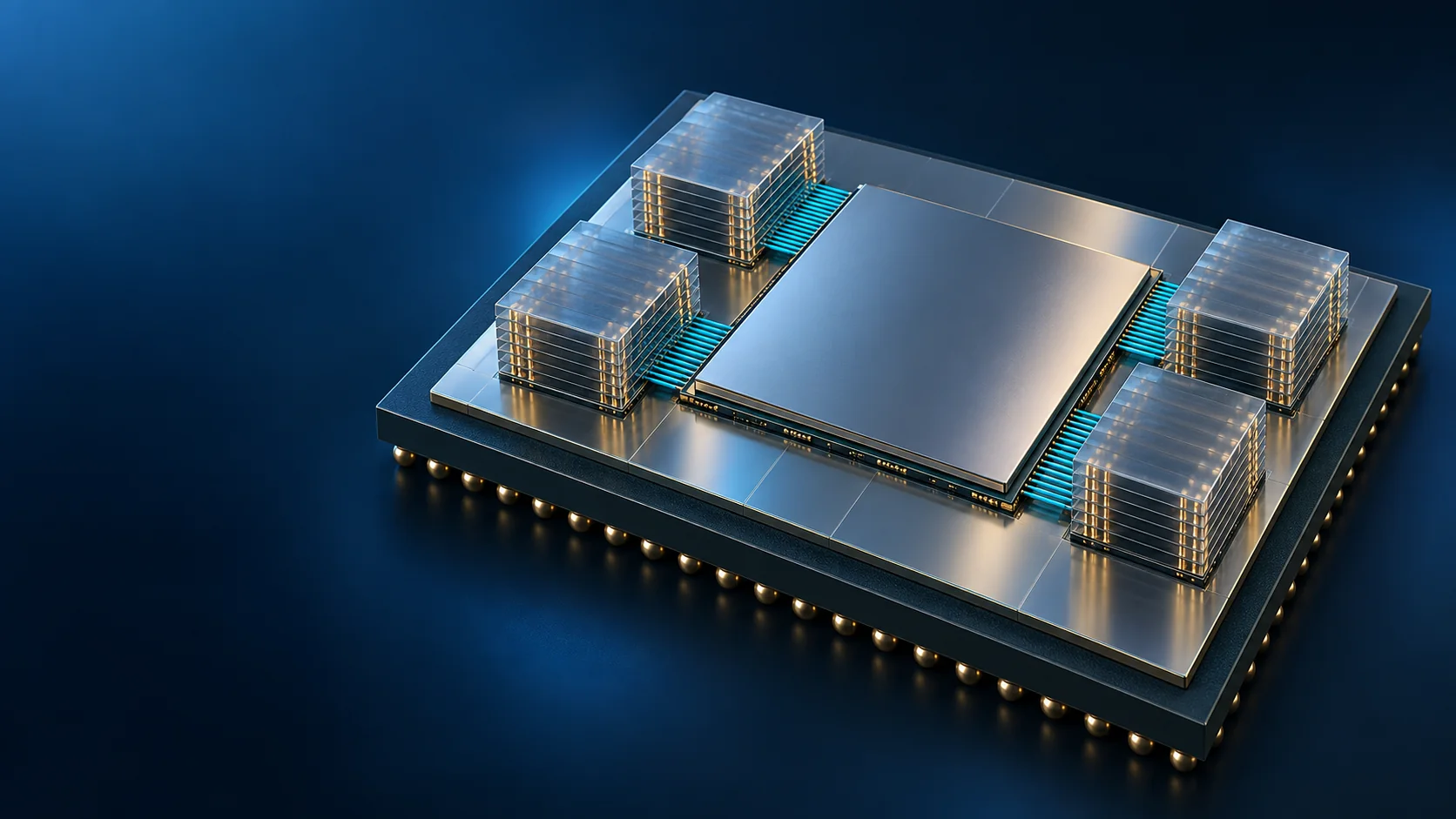
Stack DRAM vertically, sit it right beside the processor, and link the two with more than a thousand wires. This is HBM, the part that rewrote what a memory chip is allowed to look like — explained for newcomers and for materials engineers alike.
- What HBM is (the short version)
- Why HBM had to exist
- How it differs from DDR and GDDR
- Where the bandwidth actually comes from
- Structure: TSVs, microbumps, base die, interposer
- A materials engineer's view: thinning, encapsulation, warpage, heat
- Generation by generation, from HBM to HBM4
- Why it decides what an AI accelerator can do
- What is still hard: heat, yield, cost
- What comes next: HBM5, SPHBM4, hybrid bonding
- Glossary / Primary sources / Claim-to-source audit
Numbers in this field come from very different places, so each one carries a badge.
Sourced = a value stated in published material from a research institute or manufacturer (link given)
Our calculation = a figure this article derived, with the assumptions spelled out
Not yet confirmed = research-stage work with no confirmed production record
1. What HBM is (the short version)
HBM, short for High Bandwidth Memory, is in one line DRAM stacked vertically, placed right next to the processor, and wired up with an absurd number of connections. JEDEC, the international standards body for semiconductors, published the first version in 2013.
- Stack it: four to sixteen DRAM dies piled on top of one another to form a single cube
- Move it closer: not out on the board but inside the same package as the processor, millimetres away
- Widen it: 1,024 data wires, and 2,048 in HBM4Sourced (JEDEC, 2025)
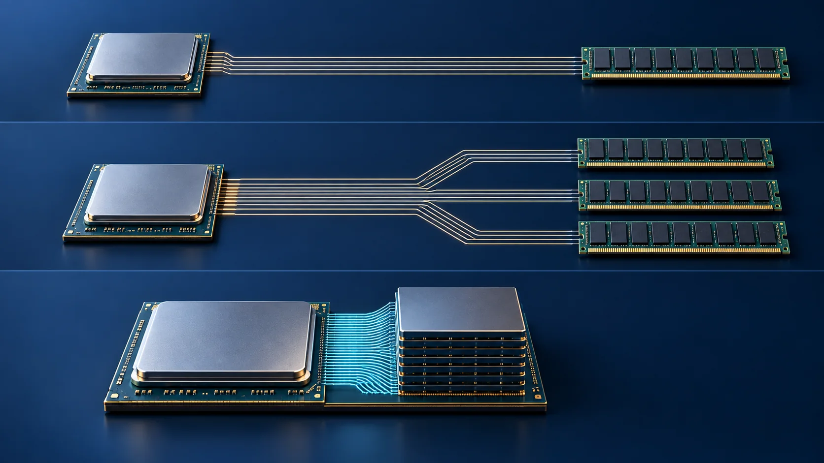
Put the three together and the HBM4 standard defines up to 2 TB/s from a single stack Sourced. One ordinary DDR5-6400 module in a PC delivers roughly 51.2 GB/sOur calculation. That is a gap of about forty times.
2. Why HBM had to exist
Compute got faster; the data stopped keeping up
A computer's performance rests on two things: how fast it can calculate, and how fast it can move data. Over the past few decades the first grew explosively while the second did not. The result is that arithmetic units finish their work and then sit waiting for the next batch of data. This is the problem known as the memory wall.
Generative AI, and large language model inference in particular, shows it in an extreme form. Every single token the model emits requires its weights to be read out of memory. Once a model runs to hundreds of gigabytes, throughput stops being a question of how fast you can compute and becomes a question of how fast you can read.
Raising the clock ran out of road
In principle there are only two ways to move more data: (A) run each wire faster, or (B) add more wires.
DDR and GDDR took route (A). But driving a trace that runs several centimetres across a printed circuit board at a high frequency degrades the signal and sends power consumption climbing. The faster each wire runs, the stronger both the transmitter and the receiver have to be, and both power and noise hit a wall.
The HBM answer: make the wires short, then win on count
HBM took route (B). Routing more than a thousand high-speed traces across a board is not physically practical, so HBM changed the premise instead.
- Stack the DRAM vertically so it takes up less area in plan view
- Put it inside the same package as the processor, cutting the wiring distance from centimetres to millimetres
- Connect through silicon wiring layers (an interposer) rather than a board, which allows thousands of traces at µm dimensions
Short wires reflect and attenuate far less, which means lower voltages and lower frequencies can still carry enormous traffic. The HBM3 standard does exactly that: a 0.4 V low-swing host interface with the supply dropped to 1.1 V Sourced (JEDEC, 2022).
GDDR is a two-lane road driven at close to the speed limit. HBM keeps the speed modest but builds 2,048 lanes. Since nobody can build a 2,048-lane road over any distance, the trick is to put the warehouse (the DRAM) directly alongside the factory (the processor) and span only a few millimetres. That is the whole idea.

3. How it differs from DDR and GDDR
| Point of comparison | DDR5 (PC and server main memory) | GDDR7 (graphics) | HBM4 |
|---|---|---|---|
| How it is mounted | DIMM module, removable | Individual packages placed on the board | Stacked inside the processor's own package |
| Distance to the processor | A few to fifteen cm | A few cm | A few mm |
| Data wires | 64 bit per module | Tens of bits per device | 2,048 bit per stack Sourced |
| Bandwidth | About 51.2 GB/s for one DDR5-6400 moduleOur calculation | Up to 192 GB/s per device Sourced | Up to 2 TB/s per stack Sourced |
| How you add capacity | Plug in more modules, into the terabyte range | Fit more devices | Fixed by stack count and layer count; cannot be added later |
| Replacement and repair | Possible | Effectively impossible once soldered down | Impossible; it is part of the package |
| Cost | Low | Moderate | High, and advanced packaging is mandatory |
| Where it is used | Main memory in PCs and servers | Gaming GPUs and consumer devices | AI accelerators and HPC |
The table scrolls sideways. The 192 GB/s figure for GDDR7 is the per-device ceiling set by JEDEC JESD239. A GPU board reaches its total by placing several devices side by side.
The point worth holding on to is that HBM is not a better DDR. You cannot add HBM capacity afterwards and it is expensive. DDR gives up bandwidth but is cheap, scales to large capacities and can be swapped out. Today's AI servers carry both, with each doing the job it is good at.
4. Where the bandwidth actually comes from
Memory bandwidth follows one very simple expression.
| Memory | Wires | Speed per wire | Bandwidth | Label |
|---|---|---|---|---|
| HBM4 (JEDEC ceiling) | 2,048 bit | 8 Gb/s | 2,048 GB/s = 2 TB/s | Sourced |
| HBM3 (JEDEC ceiling) | 1,024 bit | 6.4 Gb/s | 819 GB/s | Sourced |
| One DDR5-6400 DIMM | 64 bit | 6.4 GT/s | 51.2 GB/s | Our calculation |
Look closely and the striking thing is that HBM is barely faster per wire than DDR5: 8 Gb/s for HBM4 against 6.4 GT/s for DDR5-6400. HBM wins not because each wire is quick but because there are thirty-two times as many of them. Not faster, wider — which is exactly what the word Bandwidth in the name is pointing at.
5. Structure: TSVs, microbumps, base die, interposer
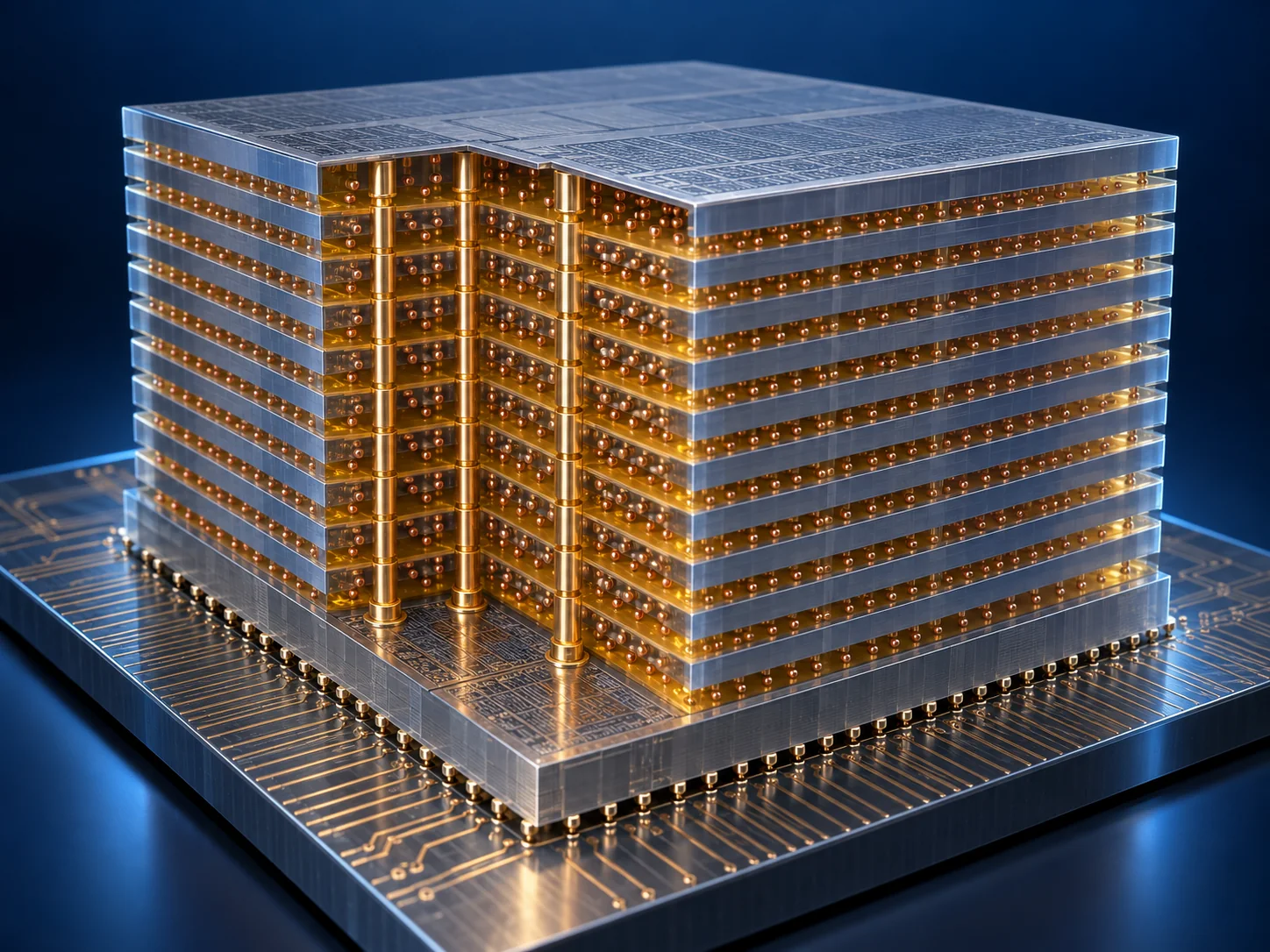
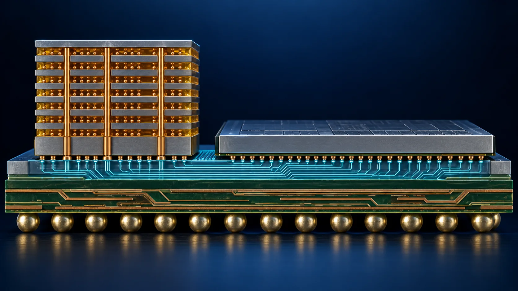
HBM is not a single component. It is a structure assembled in three dimensions out of several elements. Here they are from the bottom up.
What each part does
- DRAM core dies: the layers that actually hold the data. The JEDEC standards define 4-, 8-, 12- and 16-high configurationsSourced.
- Base die: the control chip at the bottom of the stack. It handles the external interface and the test functions.
- TSV (through-silicon via): a copper electrode that passes clean through the silicon die. Without it there is no short path between stacked chips, which makes it the element that lets HBM exist at all.
- Microbumps: the tiny joints between die and die, and between die and interposer. They are copper pillars topped with solder.
- Encapsulant: the resin filling the gaps between dies. It protects the stack mechanically and also serves as a path for heat (see section 6).
- Silicon interposer: the floor that carries both the HBM stacks and the logic die. Fine wiring on silicon is what makes thousands of connections possible.
HBM4 doubled the data wires from 1,024 to 2,048 and the independent channel count from 16 to 32Sourced (JEDEC, 2025). Doubling the wires means doubling the connection points between the base die and the interposer as well. That single change pushed the packaging difficulty up a level.
6. A materials engineer's view: thinning, encapsulation, warpage, heat
The race in HBM is, in truth, as much a race in materials and process as it is a race in DRAM circuitry. This is the part that most explanations of HBM leave out.
(1) Thinning the dies, because the height budget will not move
The total package height of HBM is fixed, so the only way to add layers is to make the DRAM chips themselves thinner. SK hynix has stated that its 12-high HBM3 uses DRAM chips 40% thinner than the 8-high partSourced (SK hynix). Samsung says its TC-NCF technology fits a 12-high part into the same package height as an 8-high oneSourced (Samsung, 2024).
Thinner silicon, naturally, warps more easily and cracks more easily. From here on, everything is a question of materials and stress.
(2) Two schools of encapsulation: MR-MUF and TC-NCF
How do you fill the gaps between stacked dies? Two broad approaches exist, and manufacturers have split between them.
| Approach | MR-MUF (mass reflow molded underfill) | TC-NCF (thermal compression with non-conductive film) |
|---|---|---|
| Process concept | Stack the dies, join every bump in one reflow, then flow in liquid encapsulant and cure it | Lay down an NCF film in advance and apply heat and pressure one layer at a time |
| Main material | EMC, a thermosetting encapsulant built on epoxy resin | NCF, a non-conductive film |
| Thermal argument | Allows up to four times as many thermal dummy bumps as TC-NCF, which help spread the heatSourced | Improves thermal behaviour by using bumps of different sizes in different placesSourced |
| Published results | The new EMC for Advanced MR-MUF dissipates heat 1.6 times better than the previous one, and HBM2E improved thermal performance by 36% over HBM2Sourced | A chip-to-chip gap of 7 µm, and more than 20% higher vertical density than an 8-high HBM3 partSourced |
| Source | SK hynix Newsroom | Samsung Newsroom |
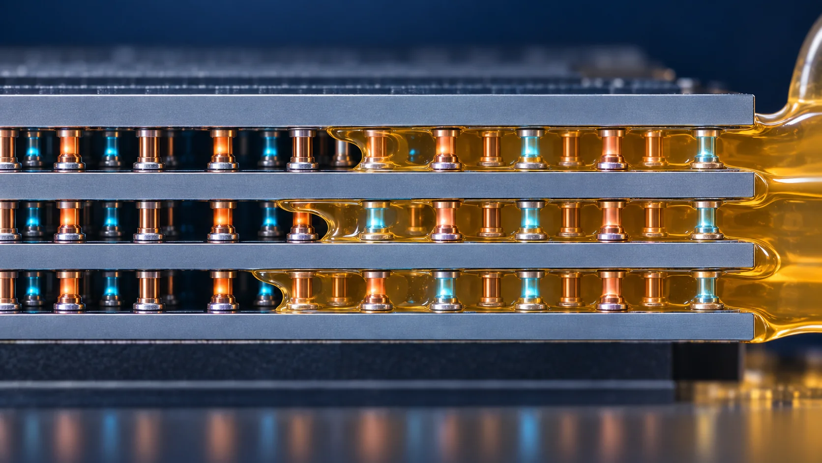
The encapsulant is not protection. It is plumbing for heat. A DRAM die in the middle of a stack has another die above it and another below it, and almost nowhere for its heat to go. There are exactly two escape routes: (a) the metal columns formed by the TSVs and the copper bumps, and (b) the resin filling the space between dies. That is precisely why SK hynix places large numbers of thermal dummy bumps that carry no electrical signal at all and why it improved the thermal conductivity of the EMC itself by a factor of 1.6.
At the same time this resin is sandwiched between materials with very different coefficients of thermal expansion: silicon, copper and an organic substrate. Cure shrinkage and thermal cycling are the main drivers of warpage and bump failure, so thermal conductivity, modulus, glass transition temperature, filler particle size and flow behaviour all have to be satisfied at once. The more layers you add and the thinner the dies get, the less room this leaves.
(3) Keeping warpage under control
SK hynix describes a chip control technique in which, at each stacking step, a brief burst of heat fuses the bumps of the upper chip to the pads of the lower one, so that those pads hold the chip in place and prevent it from warpingSourced (SK hynix). Thinning, stacking, encapsulation and warpage control are not separate problems. They are one set of simultaneous equations whose terms trade against each other.
(4) The floor itself may change: from silicon to organic substrate
HBM has always assumed a silicon interposer underneath. In June 2026, however, JEDEC published SPHBM4 (JESD330-4)Sourced. It uses the same DRAM dies as HBM4 but routes them through a new interface base die so that the stack can be mounted on an ordinary organic substrate.
The mechanism is straightforward. Where HBM4 uses 2,048 data signals, SPHBM4 reaches comparable total throughput with 512 signals and 4:1 serialisationSourced. Cutting the signal count to a quarter relaxes the bump pitch, and a relaxed pitch is what makes an organic substrate viable (JEDEC).
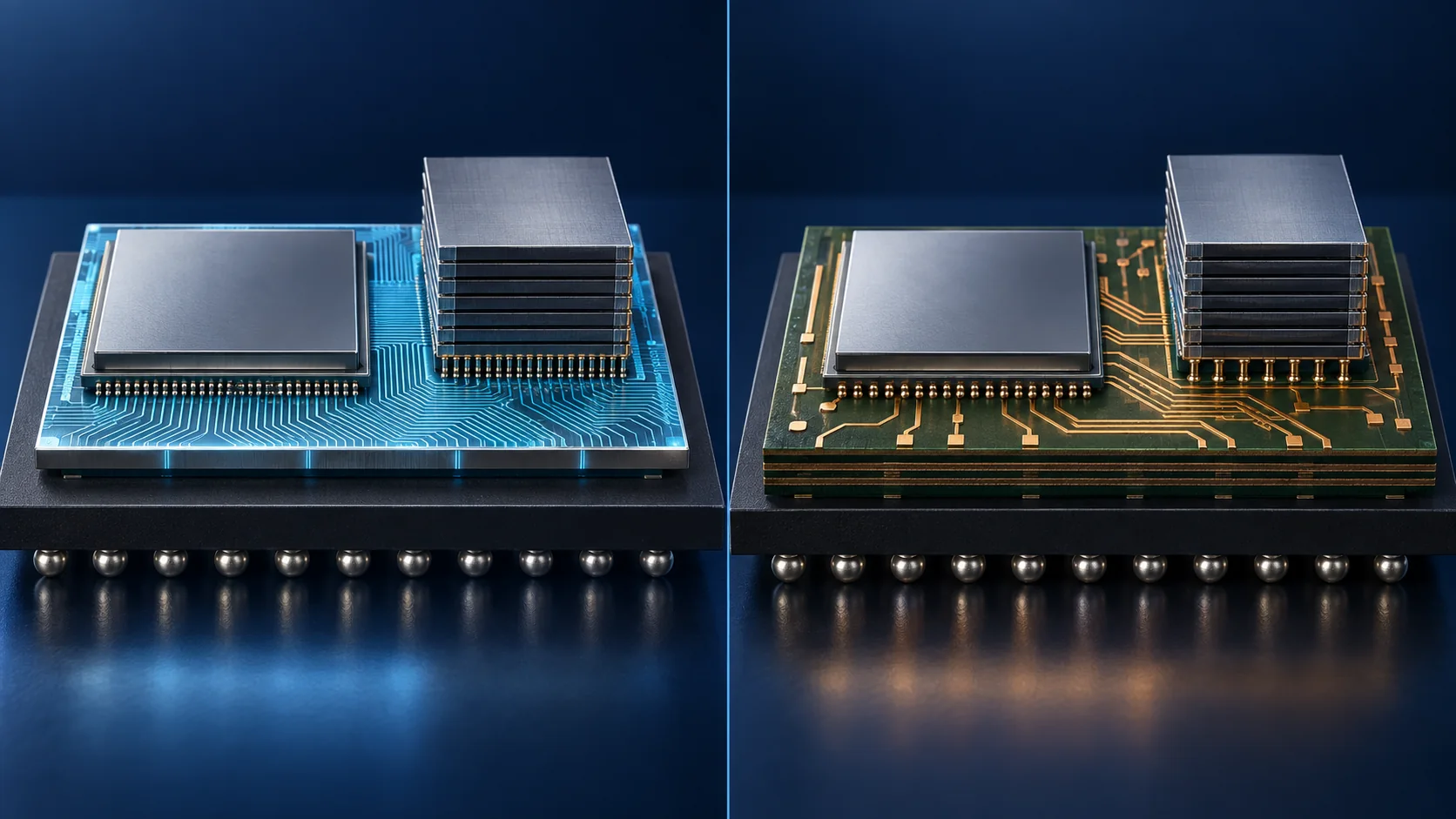
If the silicon interposer stops being mandatory, then organic substrate materials, build-up materials and fine wiring formation processes join the main battlefield of HBM assembly. For a materials supplier, SPHBM4 may turn out to matter far more than a standards document usually does.
7. Generation by generation, from HBM to HBM4
(A) How the JEDEC standards moved
| Standard | Published | I/O width | Pin speed (ceiling) | Bandwidth per stack | Layers | Capacity per stack |
|---|---|---|---|---|---|---|
| JESD235A (HBM2) | January 2016 | 1,024 bit | 2 Gb/s | 256 GB/s | 2, 4 or 8 high | 1 to 8 GB |
| JESD235B | December 2018 | 1,024 bit | 2.4 Gb/s | 307 GB/s | 2, 4, 8 or 12 high | 1 to 24 GB |
| JESD238 (HBM3) | January 2022 | 1,024 bit | 6.4 Gb/s | 819 GB/s | 4, 8 or 12 high, extensible to 16 | 4 to 64 GB |
| JESD270-4 (HBM4) | April 2025 | 2,048 bit | 8 Gb/s | 2 TB/s | 4, 8, 12 or 16 high | Up to 64 GB |
| JESD330-4 (SPHBM4) | June 2026 | 512 bit with 4:1 serialisation | — | Comparable total throughput to HBM4 | Same core dies as HBM4 | Same as HBM4 |
Every row is Sourced from JEDEC's published material. JESD270-4 was revised to JESD270-4A (Version 1.1) in December 2025.
The HBM standards JEDEC actually publishes are the JESD235 family (HBM and HBM2), the JESD238 family (HBM3), the JESD270-4 family (HBM4) and JESD330-4 (SPHBM4) (the document list on JEDEC's main memory page). There is no separate standard number called HBM2E or HBM3E. Those are vendors' own names for faster product families within a generation. Which is why a product specification can sit above the ceiling written in the standard, as the next table shows.
(B) Products and deployments
| When | Product or deployment | Headline published specification |
|---|---|---|
| 2015 | AMD Radeon R9 Fury X, the first GPU with HBM | A 4,096 bit memory interface at 512 GB/s, which works out to 1,024 bit and roughly 128 GB/s per stackOur calculation |
| July 2020 | SK hynix HBM2E in mass production | 1,024 I/O, 3.6 Gb/s per pin, over 460 GB/s, 16 GB from eight 16Gb dies |
| February 2024 | Samsung HBM3E 12H (36GB) | 12 high, 36 GB, up to 1,280 GB/s, TC-NCF, 7 µm chip-to-chip gap |
| 2024 onwards | Micron HBM3E | 8 high 24 GB and 12 high 36 GB, pin speed above 9.2 Gb/s, above 1.2 TB/s, 16 channels and 32 pseudo-channels, 1,024 I/O |
| 2024 onwards | NVIDIA H200, using HBM3E | HBM3E, 141 GB at 4.8 TB/s |
| September 2025 | SK hynix completes HBM4 development | 2,048 I/O, above 10 Gb/s and explicitly stated to exceed the 8 Gb/s in the JEDEC standard, power efficiency improved by more than 40%, 1bnm process, Advanced MR-MUF |
| 2026 | Micron HBM4 in mass production | 2,048 pins, above 11 Gb/s, above 2.8 TB/s per stack, 12 high 36 GB. A 16 high 48 GB part is sampling |
| 2026 | NVIDIA Rubin, using HBM4 | HBM4, up to 288 GB at up to 22 TB/s, 12-high stacks. NVIDIA describes the interface as twice the width of HBM3E |
All rows are Sourced from the companies' own material, listed at the end. Only the 128 GB/s per stack figure in the AMD row is a calculation by this article.
The JEDEC ceiling for HBM4 is 8 Gb/s, yet SK hynix publishes above 10 Gb/s and Micron above 11 Gb/s. SK hynix says in as many words that its part exceeds the JEDEC standard's 8 Gbps, and that is the point: a standard guarantees a floor of interoperability; it does not cap what a product may do. When a technical article quotes a number, it has to say whether it is a standard value or a product value.
8. Why it decides what an AI accelerator can do
Inference speed is a memory bandwidth question
To emit one token, an LLM must read out the model weights. At small batch sizes the amount of data read per arithmetic operation is large, so the ceiling on throughput is memory bandwidth, not the arithmetic units. Double the bandwidth in that regime and throughput moves roughly in step.
Capacity matters just as much
If the model does not fit in memory, it has to be split across several GPUs that then talk to each other, and that communication becomes the new bottleneck. HBM is one of the few ways to buy bandwidth and capacity at the same time.
What the shipping hardware shows
| Generation | Example | Memory capacity | Memory bandwidth |
|---|---|---|---|
| HBM3E | NVIDIA H200 | 141 GB | 4.8 TB/s |
| HBM4 | NVIDIA Rubin | Up to 288 GB | Up to 22 TB/s |
Both are NVIDIA's published figuresSourced. NVIDIA describes Rubin as delivering 2.8 times the bandwidth of Blackwell and Blackwell Ultra.
Divide Rubin's 22 TB/s across its 12-high stacks and you get about 2.75 TB/s per stackOur calculation, which lines up well with the above 2.8 TB/s that Micron publishes for HBM4. It confirms that an AI accelerator's bandwidth is essentially one stack's performance multiplied by the number of stacks.
9. What is still hard: heat, yield, cost
(1) Heat
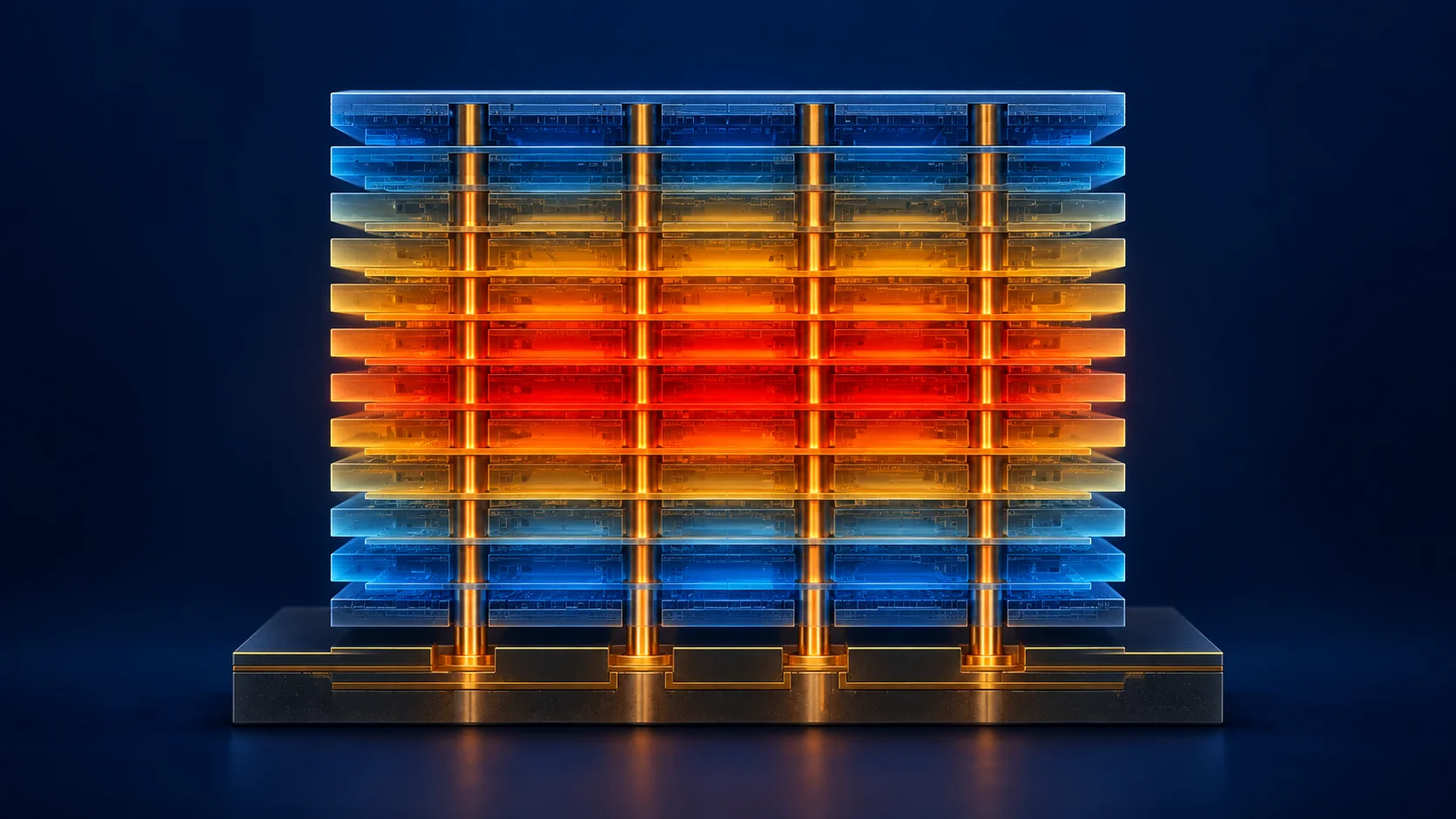
A die in the interior of a stack is sandwiched between other dies and has few routes out for its heat. More layers, thinner dies and faster operation all make this worse. The reason every manufacturer competes on encapsulant thermal conductivity and thermal dummy bump counts is that this constraint sets the real ceiling on performance.
(2) Yield
By construction, a single bad die makes the whole stack bad. A 12-high part becomes a product only if all twelve dies are good and all eleven bonding interfaces succeed. The more layers you add, the worse the final good-part rate becomes. That follows from the structure itself (this paragraph argues from structure and makes no claim about any manufacturer's yield figures).
(3) Assembly cost
HBM presupposes advanced packaging such as a silicon interposer. In TSMC's CoWoS, interposer area has grown from roughly one reticle, about 830 mm², to the 3.3-reticle classSourced (TSMC). The more large-area silicon you use, the heavier the yield and cost burden, so the cost driver is not the memory alone but the whole packaging flow. Read that way, SPHBM4 looks like the standards world's answer to a structural cost problem.
10. What comes next
HBM5: JEDEC has stated that work is under way in JC-42.2, its HBM subcommitteeSourced (JEDEC). No specification details have been published.
SPHBM4: published in June 2026. Mounting on an organic substrate now exists as a standardised optionSourced.
The technique drawing attention for pushing layer counts higher is hybrid bonding, which joins copper to copper directly with no solder bump in betweenNot yet confirmed. Removing the bump would cut the thickness between layers substantially and should help thermal conduction as well.
However, as of this article's research in September 2026 we found no official manufacturer announcement that hybrid bonding is being used in HBM volume production. Industry press takes differing views on the timing, so it should not be treated as settled. When writing about it, we would label it explicitly as a technology under study and development.
11. Glossary
- HBM
- High Bandwidth Memory. A memory standard that stacks DRAM and links it at high bandwidth inside the processor's own package.
- Bandwidth
- How much data can be moved per unit time, in GB/s or TB/s. Wire count multiplied by per-wire speed, divided by eight.
- TSV
- Through-Silicon Via. An electrode passing through a silicon die, connecting stacked chips by the shortest possible route.
- Microbump
- A tiny joint between two dies, or between a die and an interposer. A copper pillar topped with solder.
- Base die
- The control chip at the bottom of an HBM stack, handling channel control and test functions.
- Interposer
- The intermediate substrate carrying the HBM and the logic die. A silicon one allows thousands of connections in fine wiring.
- Channel and pseudo-channel
- Independently operating divisions of the memory. HBM4 has 32 channels, each with two pseudo-channels, to raise parallelism.
- EMC
- Epoxy Molding Compound. A thermosetting encapsulant based on epoxy resin, used in MR-MUF.
- NCF
- Non-Conductive Film. An adhesive film with no electrical conduction, used between layers in TC-NCF.
- MR-MUF
- Mass Reflow Molded Underfill. Joining every bump in one reflow, then filling with liquid encapsulant.
- TC-NCF
- Thermal Compression Non-Conductive Film. Bonding one layer at a time by heat and pressure through a film.
- Thermal dummy bump
- A bump that carries no electrical signal and exists purely to spread heat.
- Warpage
- Deformation of a substrate or die caused by mismatched thermal expansion or by cure shrinkage of resin. The main cause of bonding defects.
- Reticle
- The largest area a lithography tool can print in one exposure, about 830 mm². It sets the upper limit on interposer area.
- SPHBM4
- Standard Package HBM4. A JEDEC standard (JESD330-4) that cuts the signal count to 512 so the stack can be mounted on an organic substrate.
12. Primary sources
- JEDEC "JEDEC and Industry Leaders Collaborate to Release JESD270-4 HBM4 Standard", 16 April 2025 — jedec.org
- JEDEC "High Bandwidth Memory (HBM4) DRAM / JESD270-4A", December 2025 — jedec.org
- JEDEC "JEDEC Publishes HBM3 Update to High Bandwidth Memory (HBM) Standard", 27 January 2022 — jedec.org
- JEDEC "JEDEC Updates Groundbreaking High Bandwidth Memory (HBM) Standard" (JESD235A), 12 January 2016 — jedec.org
- JEDEC "JEDEC Updates Groundbreaking High Bandwidth Memory (HBM) Standard" (JESD235B), 17 December 2018 — jedec.org
- JEDEC "JEDEC Prepares SPHBM4 Standard to Deliver HBM4-Level Throughput with Reduced Pin Count", 11 December 2025 — jedec.org
- JEDEC "Main Memory: DDR SDRAM, HBM" (records the June 2026 publication of JESD330-4 and the HBM5 work in progress) — jedec.org
- JEDEC "JEDEC Publishes GDDR7 Graphics Memory Standard" (JESD239), 5 March 2024 — jedec.org
- AMD "AMD Ushers in a New Era of PC Gaming with Radeon R9 and R7 300 Series", 16 June 2015 — ir.amd.com
- SK hynix "SK hynix Starts Mass-Production of High-Speed DRAM, HBM2E" — news.skhynix.com
- SK hynix "SK hynix Completes World's First HBM4 Development and Readies Mass Production", 12 September 2025 — news.skhynix.com
- SK hynix "Rulebreakers' Revolutions: MR-MUF Unlocks HBM Heat Control" — news.skhynix.com
- Samsung "Samsung Develops Industry-First 36GB HBM3E 12H DRAM", 27 February 2024 — news.samsung.com
- Micron "HBM3E" product page — micron.com
- Micron "HBM4" product page — micron.com
- NVIDIA "H200 Tensor Core GPU" — nvidia.com
- NVIDIA "Inside NVIDIA Rubin GPU Architecture" — developer.nvidia.com
- TSMC "CoWoS" technology page — 3dfabric.tsmc.com
13. Claim-to-source audit
Every significant number in this article, with where it appears, what it rests on and how it is labelled.
| Claim in the text | Basis | Label |
|---|---|---|
| HBM4 is 2,048 bit at 8 Gb/s for up to 2 TB/s, with 32 channels, 4/8/12/16 high, up to 64 GB | JEDEC JESD270-4 press release, 16 April 2025[Source 1] https://www.jedec.org/news/pressreleases/jedec%C2%AE-and-industry-leaders-collaborate-release-jesd270-4-hbm4-standard-advancing | Sourced |
| HBM3 is 1,024 bit at 6.4 Gb/s for 819 GB/s, with 16 channels and 32 pseudo-channels, 4 to 64 GB, a 0.4 V low-swing interface and 1.1 V operation | JEDEC JESD238 press release, 27 January 2022[Source 3] https://www.jedec.org/news/pressreleases/jedec-publishes-hbm3-update-high-bandwidth-memory-hbm-standard | Sourced |
| JESD235A is 1,024 bit, up to 256 GB/s and up to 8 GB | JEDEC press release, 12 January 2016[Source 4] https://www.jedec.org/news/pressreleases/jedec-updates-groundbreaking-high-bandwidth-memory-hbm-standard | Sourced |
| JESD235B reaches 2.4 Gb/s and 307 GB/s, up to 24 GB, with 12-high support | JEDEC press release, 17 December 2018[Source 5] https://www.jedec.org/news/pressreleases/jedec-updates-groundbreaking-high-bandwidth-memory-hbm-standard-0 | Sourced |
| SPHBM4 uses 512 signals with 4:1 serialisation to allow mounting on an organic substrate, and was published in June 2026 | JEDEC press release of 11 December 2025, and the JEDEC main memory page[Source 6] https://www.jedec.org/news/pressreleases/jedec%C2%AE-prepares-sphbm4-standard-deliver-hbm4-level-throughput-reduced-pin-count | Sourced |
| GDDR7 reaches up to 192 GB/s per device | JEDEC JESD239 press release, 5 March 2024[Source 8] https://www.jedec.org/news/pressreleases/jedec-publishes-gddr7-graphics-memory-standard | Sourced |
| One DDR5-6400 DIMM delivers about 51.2 GB/s | Our calculation: 64 bit multiplied by 6.4 GT/s, divided by 8 | Our calculation |
| Radeon R9 Fury X has a 4,096 bit interface at 512 GB/s, which is about 128 GB/s per stack | AMD press release, 16 June 2015. The per-stack value is 512 divided by 4, our calculation[Source 9] https://ir.amd.com/news-events/press-releases/detail/619/amd-ushers-in-a-new-era-of-pc-gaming-with-radeontm-r9-and-r7-300-series-graphics-line-up-including-worlds-first-graphics-family-with-revolutionary-hbm-technology | Sourced |
| SK hynix HBM2E runs at 3.6 Gb/s for over 460 GB/s at 16 GB | SK hynix Newsroom[Source 10] https://news.skhynix.com/sk-hynix-starts-mass-production-of-high-speed-dram-hbm2e/ | Sourced |
| Samsung HBM3E 12H is 36 GB at up to 1,280 GB/s, with a 7 µm chip-to-chip gap and more than 20% higher vertical density | Samsung Newsroom, 27 February 2024[Source 13] https://news.samsung.com/global/samsung-develops-industry-first-36gb-hbm3e-12h-dram | Sourced |
| Micron HBM3E exceeds 9.2 Gb/s and 1.2 TB/s, at 24 or 36 GB with 1,024 I/O | Micron product page[Source 14] https://www.micron.com/products/memory/hbm/hbm3e | Sourced |
| Micron HBM4 exceeds 11 Gb/s and 2.8 TB/s at 12 high 36 GB, with a 16 high 48 GB part sampling | Micron product page[Source 15] https://www.micron.com/products/memory/hbm/hbm4 | Sourced |
| SK hynix HBM4 exceeds 10 Gb/s, above the JEDEC 8 Gb/s, with power efficiency improved by more than 40%, on 1bnm and Advanced MR-MUF | SK hynix Newsroom, 12 September 2025[Source 11] https://news.skhynix.com/sk-hynix-completes-worlds-first-hbm4-development-and-readies-mass-production/ | Sourced |
| 12-high HBM3 thins the DRAM chip by 40% against the 8-high part; thermal dummy bumps up to four times the TC-NCF count; the new EMC dissipates heat 1.6 times better than the previous one; HBM2E improved 36% over HBM2 | SK hynix Newsroom, the MR-MUF explainer[Source 12] https://news.skhynix.com/rulebreaker-revolutions-mr-muf-unlocks-hbm-heat-control/ | Sourced |
| NVIDIA H200: 141 GB at 4.8 TB/s | NVIDIA product page[Source 16] https://www.nvidia.com/en-us/data-center/h200/ | Sourced |
| NVIDIA Rubin: up to 288 GB at up to 22 TB/s, in 12-high stacks | NVIDIA technical blog[Source 17] https://developer.nvidia.com/blog/inside-nvidia-rubin-gpu-architecture-powering-the-era-of-agentic-ai/ | Sourced |
| Rubin delivers about 2.75 TB/s per stack | Our calculation: 22 TB/s divided by 8 stacks, where the stack count is 288 GB divided by 36 GB | Our calculation |
| CoWoS interposers have grown from roughly one reticle, about 830 mm², to the 3.3-reticle class | TSMC CoWoS technology page[Source 18] https://3dfabric.tsmc.com/english/dedicatedFoundry/technology/cowos.htm | Sourced |
| HBM5 is in development in JEDEC JC-42.2 | JEDEC main memory page[Source 7] https://www.jedec.org/category/technology-focus-area/main-memory-ddr-sdram | Sourced |
| Hybrid bonding adopted for HBM volume production | No official manufacturer announcement was confirmed at the time of this article's research, so the outlook is left open | Not yet confirmed |
| That yield falls as layer count rises, and that the encapsulant matters as a heat path | Commentary arguing from structure. No specific numerical claim is made | Commentary |
Last updated 20 September 2026. Sources are limited to primary material: JEDEC's published standards documentation, official manufacturer announcements and product pages. All figures are explanatory concept graphics. Visual-overview figures are shown as AI-generated conceptual images, matching the Japanese edition. Vector drawings are retained where they carry quantitative values or precision-critical technical labels. AI-generated images do not depict real equipment, products, facilities, dimensions or exact cross-sections; replaced source SVG overview drawings remain in the HTML but are hidden.