TECHNOLOGY EXPLAINER
What an OSAT Is
— the companies that own the back end, and a dividing line that is starting to blur
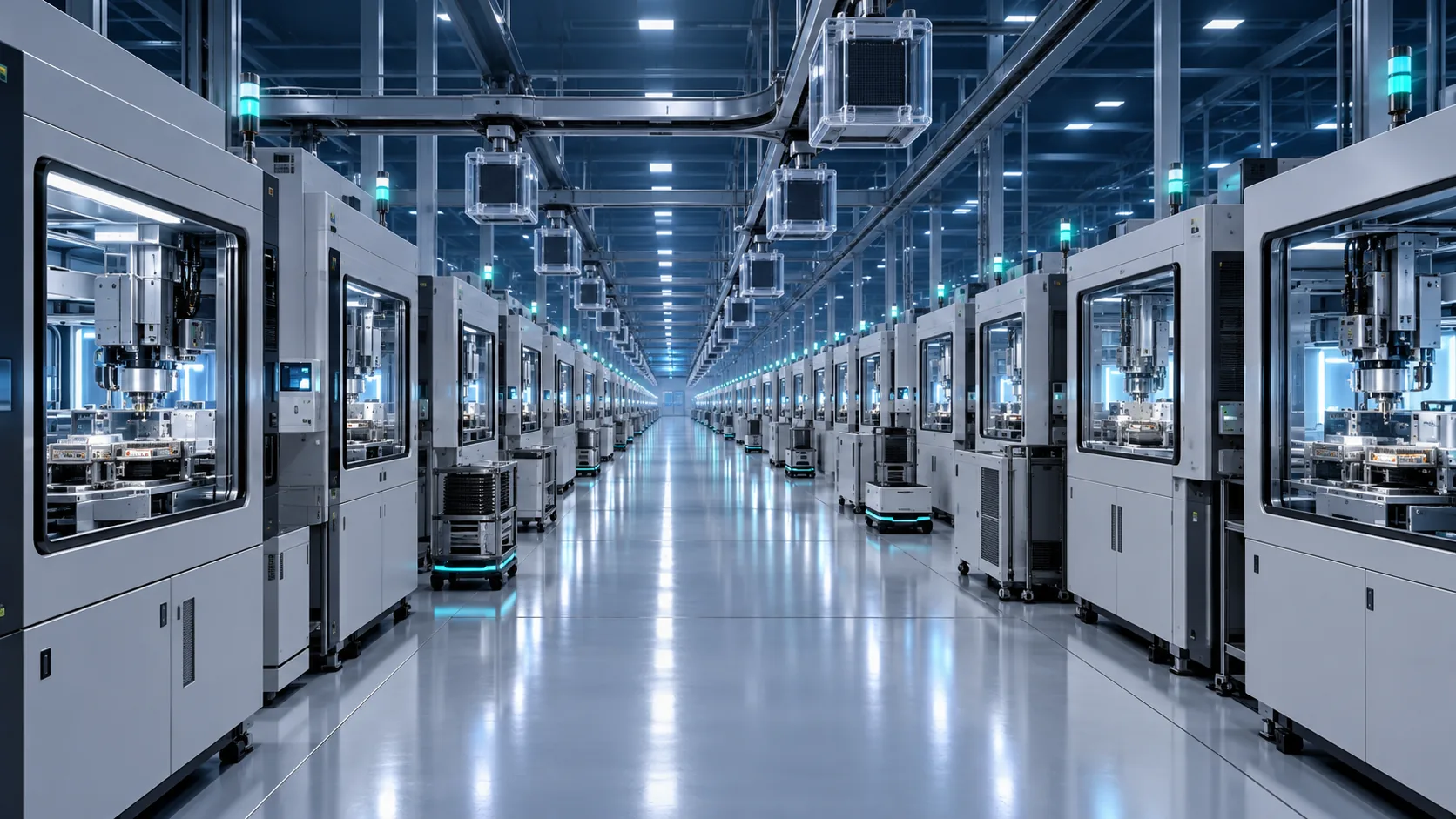
For decades, the companies that made semiconductors and the companies that assembled them were two separate worlds. Advanced packaging for AI is now rearranging that split. For a materials supplier, this is not abstract industry news: it changes who you actually sell to.
- What an OSAT is (the short version)
- Why the split happened in the first place
- What an OSAT actually does for you
- The line starts to blur — TSMC and Amkor sign a ten-year deal
- A materials engineer's view: who chooses the material?
- The map is being redrawn
- What is still hard
- Glossary / Primary sources / Claim-to-source audit
Sourced = stated in a company's own published material (link given)
Our calculation = a figure this article derived, with the assumptions spelled out
Not yet confirmed = announced plans with no confirmed track record
Structural readings and industry interpretation are marked separately as Commentary.
1. What an OSAT is (the short version)
OSAT stands for Outsourced Semiconductor Assembly and Test. In plain terms, it is a company whose whole business is assembling and testing other people's chips.
- What it takes on: receiving wafers, dicing them, mounting the dies into packages, testing them and shipping.
- Who it works for: fabless design houses, IDMs (companies that both design and manufacture), and increasingly foundries.
- Why anyone outsources it: back-end work needs different equipment and different process know-how from front-end work, and owning it outright is a heavy fixed cost.
Amkor describes itself as the largest US-headquartered OSAT and a global leader in outsourced semiconductor packaging and test servicesSourced. ASE describes itself as a leading provider of semiconductor packaging and test servicesSourced.
2. Why the split happened in the first place
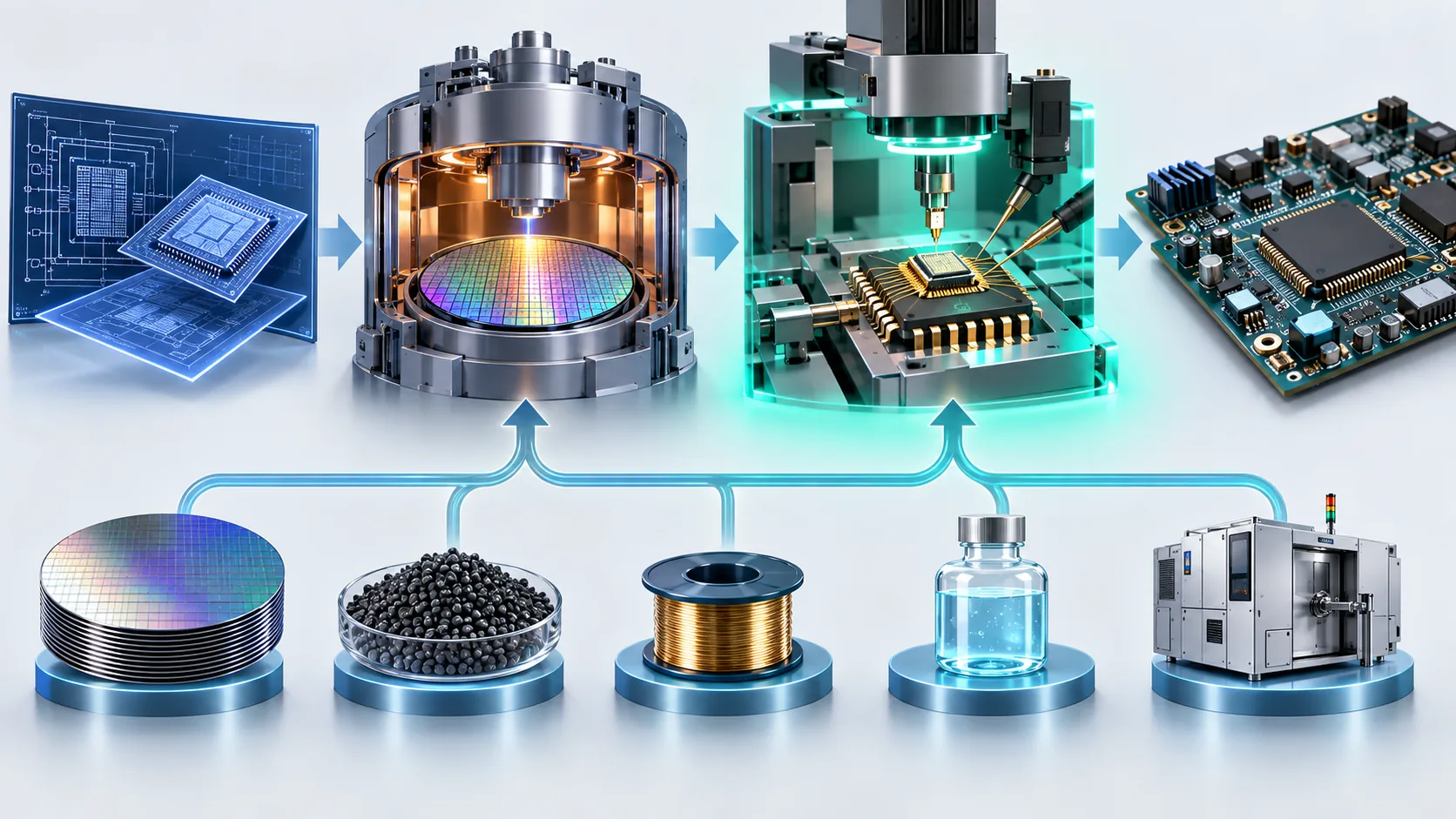
Semiconductor manufacturing divides into the front end and the back end. The front end builds circuits onto a wafer. The back end cuts that wafer up and turns the pieces into products you can solder down.
These two halves need different equipment, work at different dimensions, and demand different levels of cleanliness. A company that has already sunk enormous capital into the front end gains little by also owning a back end with a completely different character. So a class of companies emerged that does nothing but the back end.
Design and manufacturing separated, and foundries appeared. Then manufacturing itself separated into front end and back end, and OSATs appeared. It is easiest to read this as outsourcing applied twice.
3. What an OSAT actually does for you
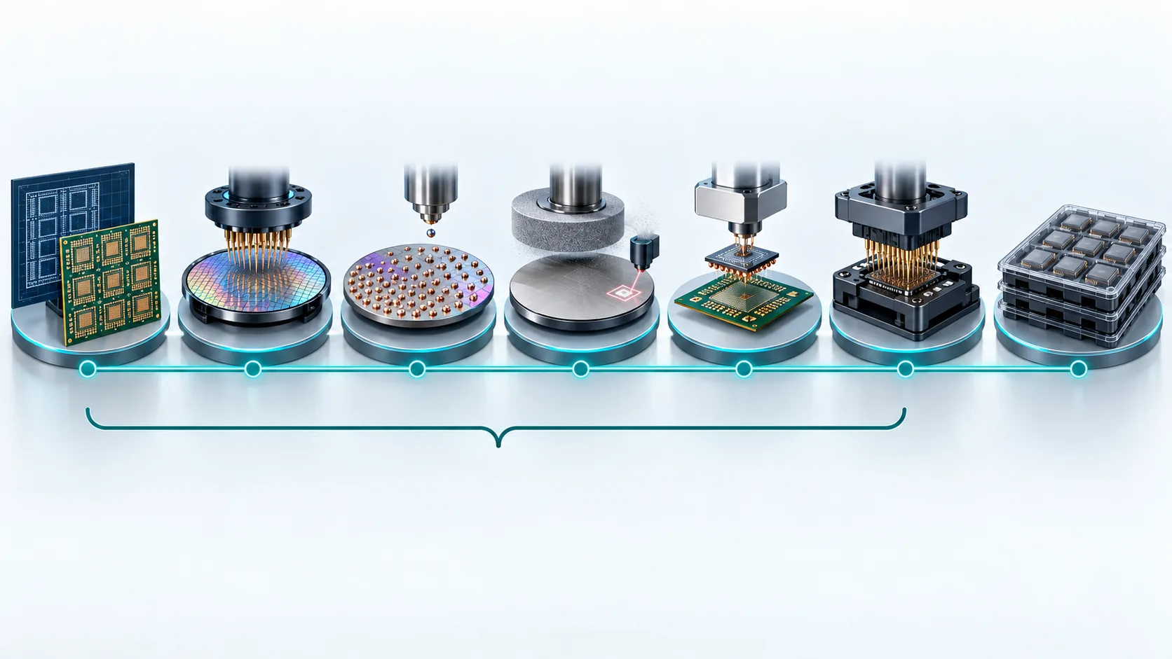
In its description of bumping services, ASE sets out the span of what it offersSourced.
Combined with other ASE manufacturing services such as substrate design, substrate manufacturing, wafer sort, bumping, backgrinding, backside marking, flip chip assembly and final test, the company says it offers customers an unparalleled turnkey solution in flip chip and wafer level packaging (ASE).
ASE was founded in 1984 and publishes a worldwide headcount of 48,000 employees across more than 50 smart factoriesSourced. It also positions itself as a leading architect of heterogeneous integration (HI), which it defines as the integration of separately manufactured components into a higher-level assembly (System-in-Package) that, in the aggregate, provides enhanced functionality and improved operating characteristicsSourced.
It is almost word for word the definition of heterogeneous integration used by the IEEE EPS Heterogeneous Integration Roadmap (HIR), which we quoted in the Heterogeneous Integration article. The HIR is a roadmap supported jointly by IEEE EPS, SEMI and IEEE EDS. In other words, an OSAT has adopted the industry's shared definition as its own banner. The self-description is deliberate: not a subcontractor, but an owner of integration technology.
4. The line starts to blur — TSMC and Amkor sign a ten-year deal
This is the part of the picture that is moving fastest.
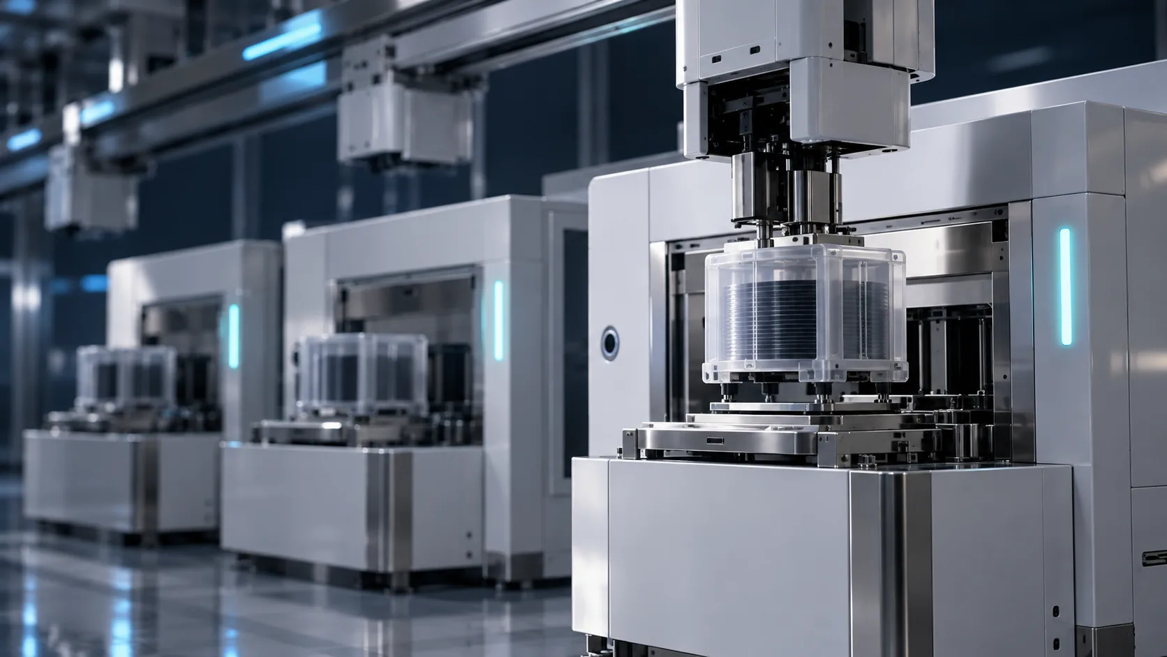
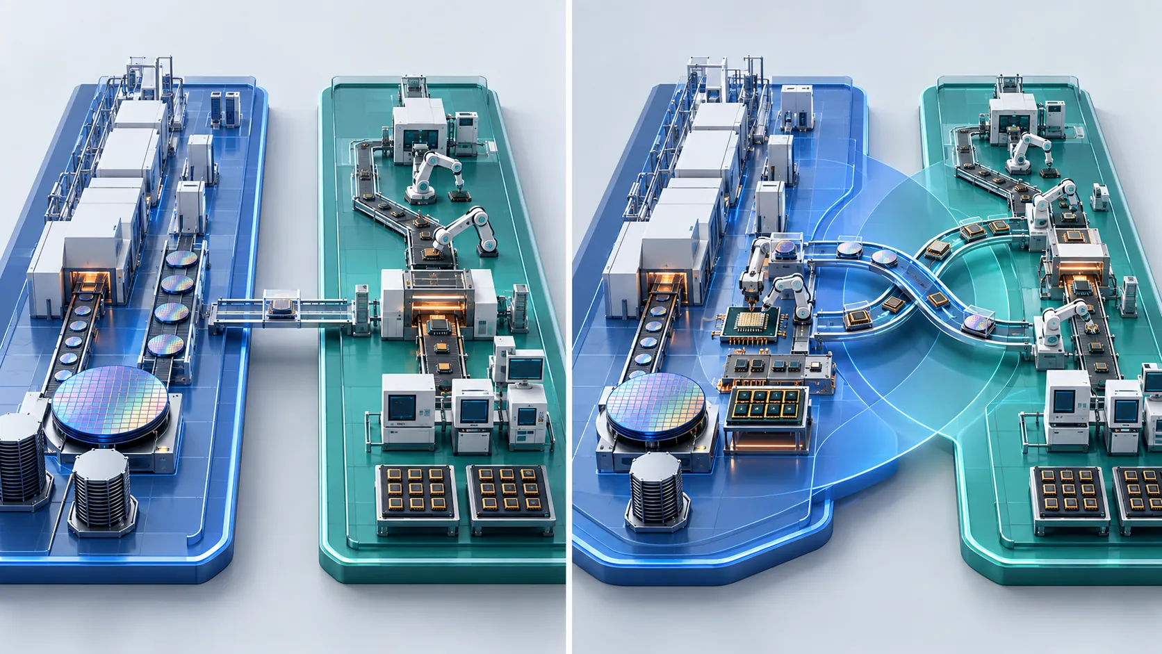
In advanced packaging for AI, foundries began doing back-end work themselves. TSMC's CoWoS is the obvious example; the company has been in volume production on that platform since 2012Sourced (covered in detail in the CoWoS article).
And yet on 16 June 2026, TSMC and Amkor announced a ten-year agreementSourced.
The two companies signed a ten-year agreement to strengthen advanced semiconductor packaging capability in Arizona. The agreement establishes a collaboration framework for TSMC to procure advanced packaging and test services from AmkorSourced.
Kevin Zhang of TSMC (Senior Vice President and Deputy Co-COO) said the company has a long history of collaborating with Amkor globally on advanced packaging, and Amkor CEO Kevin Engel said the partnership provides customers a complete US supply chain from advanced silicon manufacturing to tested packaged devicesSourced (Amkor, 16 June 2026).
5. A materials engineer's view: who chooses the material?
On the surface this is a story about industry consolidation. Seen from the materials side, it has a much more immediate meaning.
Molding compounds, substrates, underfills, temporary bonding adhesives, plating chemistries — who selects them and who buys them depends on who owns the back-end step.
If an OSAT owns it: the qualification decision sits with the OSAT, and the OSAT is your commercial counterpart.
If a foundry owns it: the decision moves to the foundry, and front-end procurement standards and quality requirements come with it.
If the design house specifies it: the decision is made upstream of whoever physically uses the material.
The boundary shift in Section 4 therefore means something concrete for a materials supplier: the question of who you call on is in motion.
An OSAT is a customer and a manufacturer at the same time
There is a further wrinkle: OSATs build some of the parts themselves. As Section 3 showed, ASE includes substrate design and substrate manufacturing in its own service listSourced.
For a materials supplier, an OSAT is simultaneously a large customer and, for parts such as substrates, an organisation that makes the thing itself.
That makes a pure sell-the-material relationship hard to sustain. As the Package Substrate and PLP articles describe, Resonac has built a consortium (JOINT3) in which materials, equipment and design tools are developed together — which reads, among other things, as a response to exactly this structureSourced.
You propose a process, not a product. Back-end materials businesses tend toward co-development because of who the customers are.
6. The map is being redrawn
Back-end capacity has long been concentrated in Taiwan, mainland China and Southeast Asia. Large North American investments are now being added on top of that.
Amkor's Arizona campus
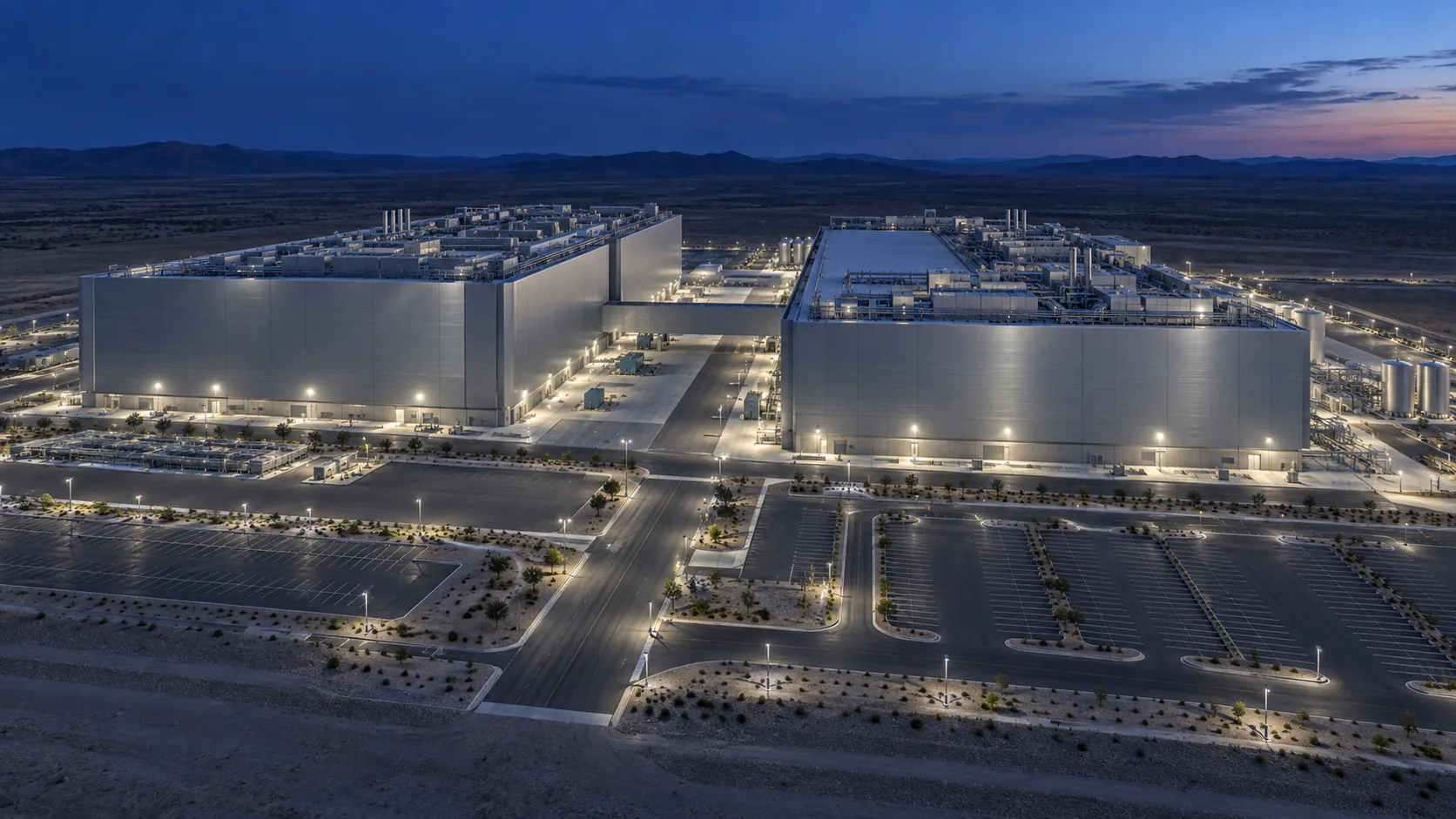
On 6 October 2025 Amkor announced the groundbreaking of a new Arizona campus and an expanded investmentSourced.
| Item | As announced |
|---|---|
| Investment | USD 7 billion across two phases (an increase of more than USD 5 billion on the earlier plan) |
| Position | The first high-volume advanced packaging facility in the United States |
| Scale | More than 750,000 square feet of cleanroom and up to 3,000 jobs when both phases are complete |
| Timing | First building due to be completed in mid-2027, with production starting in early 2028 |
| Customers | Will support major customers including Apple and NVIDIA |
| Role | Complements TSMC's front-end wafer manufacturing to enable end-to-end semiconductor manufacturing |
| Support | Backed by the CHIPS for America programme, the advanced manufacturing investment credit, and state and local support |
All rows Sourced (Amkor, 6 October 2025).
Amkor's Arizona campus is in the same region as TSMC's Arizona fab. The June 2026 announcement of the ten-year agreement also refers to the proximity of TSMC's front-end fab and Amkor's back-end facilitySourced.
That matters for material supply as well. If the back end moves to a new location, the logistics that feed it have to move too. As the Build-up Film article notes, Ajinomoto explicitly cited business continuity planning in announcing the land acquisition for a new plant — the geography of the supply network is now part of a materials supplier's investment caseSourced.
7. What is still hard
(1) The capital burden of advanced packaging
Back-end work used to require far less capital than the front end. At the level of CoWoS or hybrid bonding, it now demands tools and cleanliness close to front-end standards (see the Hybrid Bonding article). Amkor's Arizona investment reaching USD 7 billion is the clearest possible illustration of that shiftSourced.
(2) Deciding how much to own
For foundries and OSATs alike, the question of which technologies to own and which to hand over has become harder. TSMC running CoWoS in-house while simultaneously signing a ten-year agreement with Amkor suggests that the answer is being settled technology by technology and region by regionSourced.
(3) People and ramp-up
A new building in a new place does not become a production line on its own. Amkor's figure of up to 3,000 jobs is, read the other way round, a statement of how many trained people the site will needSourced.
8. Glossary
- OSAT
- Outsourced Semiconductor Assembly and Test. A company that takes on chip assembly and test under contract.
- Front end
- The steps that build circuits onto a wafer. The foundry's domain.
- Back end
- Dicing the wafer, mounting dies into packages and testing them.
- Foundry
- A company that manufactures chips to order. It does not design them.
- IDM
- Integrated Device Manufacturer. A company that both designs and manufactures its own chips.
- Turnkey
- Taking on a whole chain of steps and handing back a finished product.
- Wafer probing
- Electrically testing each die while it is still part of the wafer.
- Final test
- Electrical test carried out after the die has been packaged.
- Bumping
- Forming the connection bumps on the wafer.
- Backgrinding
- Grinding the back of the wafer to thin it.
- Flip chip
- Mounting a die face down so its bumps meet the substrate directly.
- Heterogeneous integration (HI)
- Integrating separately manufactured components into a higher-level assembly.
- SiP
- System-in-Package. Several components housed in a single package.
- BCP
- Business continuity planning. Keeping supply running through disruption.
9. Primary sources
- Amkor "TSMC and Amkor Technology Announce Long Term Partnership to Accelerate Advanced Packaging in the United States", 16 June 2026 — ir.amkor.com
- Amkor "Amkor Technology Breaks Ground on New Semiconductor Advanced Packaging and Test Campus in Arizona; Expands Investment to $7 Billion", 6 October 2025 — ir.amkor.com
- ASE "About ASE" — ase.aseglobal.com
- ASE "Bumping Services" — ase.aseglobal.com
- TSMC CoWoS technology page — 3dfabric.tsmc.com
- Resonac "27 companies establish JOINT3, a consortium for next-generation semiconductor packages" (Japanese-language release), 3 September 2025 — resonac.com
- Ajinomoto "Ajinomoto Co. and Ajinomoto Fine-Techno acquire a site for a new plant" (Japanese-language release), 7 May 2026 — news.ajinomoto.co.jp
- IEEE EPS "Heterogeneous Integration Roadmap" — eps.ieee.org
10. Claim-to-source audit
| Claim in the text | Basis | Label |
|---|---|---|
| Amkor describes itself as the largest US-headquartered OSAT and a global leader in outsourced semiconductor packaging and test services | Amkor press release, 16 June 2026[Source 1] https://ir.amkor.com/news-releases/news-release-details/tsmc-and-amkor-technology-announce-long-term-partnership | Sourced |
| TSMC and Amkor signed a ten-year agreement establishing a framework for TSMC to procure advanced packaging and test services from Amkor; the quoted statements from both executives; the proximity of the front-end fab and the back-end facility | Amkor press release, 16 June 2026[Source 1] https://ir.amkor.com/news-releases/news-release-details/tsmc-and-amkor-technology-announce-long-term-partnership | Sourced |
| Amkor Arizona: USD 7 billion total investment (an increase of more than USD 5 billion), the first high-volume advanced packaging facility in the United States, more than 750,000 square feet of cleanroom, up to 3,000 jobs, first building mid-2027 with production in early 2028, customers including Apple and NVIDIA, complementing TSMC's front-end manufacturing, supported by CHIPS for America and related programmes | Amkor press release, 6 October 2025[Source 2] https://ir.amkor.com/news-releases/news-release-details/amkor-technology-breaks-ground-new-semiconductor-advanced | Sourced |
| ASE describes itself as a leading provider of semiconductor packaging and test services; founded 1984; 48,000 employees; more than 50 smart factories; positions itself as a leading architect of heterogeneous integration and publishes the HI definition quoted here | ASE "About ASE"[Source 3] https://ase.aseglobal.com/about-ase/ | Sourced |
| ASE lists substrate design, substrate manufacturing, wafer sort, bumping, backgrinding, backside marking, flip chip assembly and final test among its services, and describes an unparalleled turnkey solution in flip chip and wafer level packaging | ASE "Bumping Services"[Source 4] https://ase.aseglobal.com/bumping-services/ | Sourced |
| TSMC has been in volume production on CoWoS since 2012 | TSMC CoWoS technology page[Source 5] https://3dfabric.tsmc.com/english/dedicatedFoundry/technology/cowos.htm | Sourced |
| Resonac develops materials, equipment and design tools jointly through the JOINT3 consortium | Resonac news release, 3 September 2025[Source 6] https://www.resonac.com/jp/news/2025/09/03/3596.html | Sourced |
| Ajinomoto's announcement of a new plant site cites business continuity planning | Ajinomoto news release, 7 May 2026[Source 7] https://news.ajinomoto.co.jp/2026/05/20260507-02.html | Sourced |
| ASE's definition of heterogeneous integration is nearly identical to the IEEE EPS HIR definition | Comparison of the wording in ASE "About ASE" and IEEE EPS / HIR[Source 3] https://ase.aseglobal.com/about-ase/[Source 8] https://eps.ieee.org/technology/heterogeneous-integration-roadmap/ | Sourced |
| Why the front-end/back-end split emerged; the argument that the owner of a step determines who qualifies a material; the observation that back-end materials businesses tend toward co-development; the reading in Fig. 4 that companies are re-deciding what to keep in-house | Commentary by this article based on published material. Not an industry taxonomy, and not a strategy stated by any of the companies | Commentary |
Last updated 20 September 2026. Sources are limited to primary material (company announcements and corporate information pages). This article includes structural interpretation of the industry, which is separated out as Commentary and distinguished from sourced fact. All figures are explanatory concept graphics. Visual-overview figures are shown as AI-generated conceptual images, matching the Japanese edition. Vector drawings are retained where they carry quantitative values or precision-critical technical labels. AI-generated images do not depict real equipment, products, facilities, dimensions or exact cross-sections; replaced source SVG overview drawings remain in the HTML but are hidden.