TECHNOLOGY EXPLAINER
What Panel Level Packaging (PLP) Is
— giving up the round wafer and building on a square sheet
Semiconductors have been built on round wafers for decades. But in packaging, being round is a disadvantage. This article covers the idea of building on large rectangular panels, like display glass, and the materials problem standing in the way.
- What PLP is (the short version)
- Why rectangular — you cannot tile a circle with squares
- Standardising the panel size (SEMI 3D20)
- The central technical problem: die shift
- A materials engineer's view: the combination decides the result
- Activity in Japan: Resonac's JOINT3
- What is still hard
- Glossary / Primary sources / Claim-to-source audit
Sourced = a value stated in published material from a standards body, research institute or manufacturer (link given)
Our calculation = a figure this article derived, with the assumptions spelled out
Not yet confirmed = a plan or target with no confirmed production record
1. What PLP is (the short version)
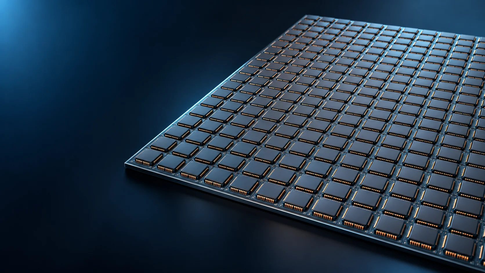
Panel Level Packaging means building semiconductor packages together on a large rectangular panel instead of on a round wafer.
- A different surface: not a 300 mm circle, but a rectangle such as 510 x 515 mm
- The same products: fan-out packages and interposers
- The point is throughput: more units per processing run, and therefore a lower cost per unit
Building fan-out packages on a wafer is FOWLP (Fan-Out Wafer Level Packaging); building them on a panel is FOPLP (Fan-Out Panel Level Packaging).
The RDL article dealt with wiring layers built directly onto the die. PLP is about the shape of the surface those steps are carried out on. It does not change what you build; it changes the shape of the place you build it — a manufacturing idea rather than a device idea.
2. Why rectangular — you cannot tile a circle with squares
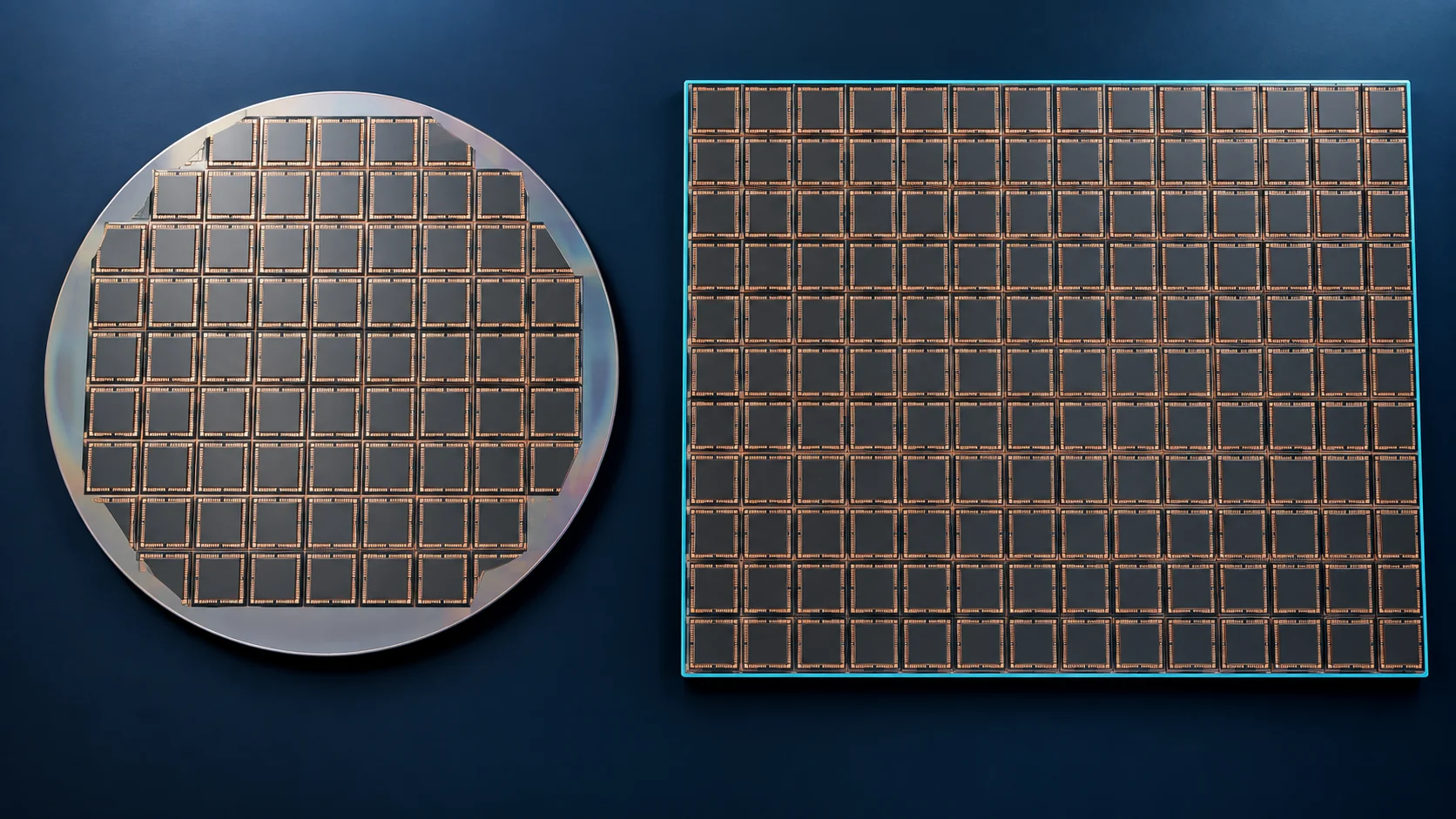
The reason is geometric. Cut squares from a round surface and the rim is always wasted. And the larger the square you are cutting, the worse that waste becomes.
The bigger the package, the wider the gap
Repeating the same calculation for different package sizes makes the trend obvious.
| Package size | 300 mm wafer | 510 x 515 mm panel | Units per sheet, ratio | Wafer area used |
|---|---|---|---|---|
| 25 mm square | 93 | 400 | 4.30x | 82% |
| 50 mm square | 21 | 100 | 4.76x | 74% |
| 75 mm square | 7 | 36 | 5.14x | 56% |
All rows Our calculation. The area ratio is fixed at 3.72x, yet the ratio of units per sheet climbs from 4.30x to 5.14x. The difference is the waste around the rim of the circle.
The table is the whole answer. The larger the package, the worse the round wafer performs. At 75 mm square the wafer's area utilisation is 56% — close to half of it thrown away.
And packages for AI are getting larger right now (as the CoWoS article shows, interposers are planned out to 14 reticles, equivalent to roughly 108 mm square). Every increase in package size strengthens the case for PLP — which is why a technology that sat in research for years has suddenly become urgent.
3. Standardising the panel size (SEMI 3D20)
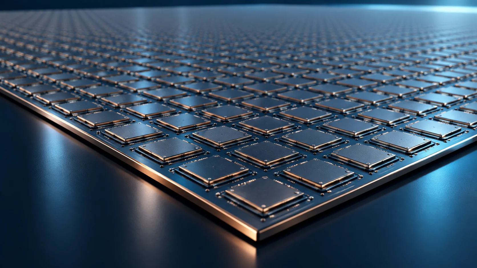
PLP had a problem that came before any technical one: every company was developing on a different panel size.
A SEMI blog post of 28 August 2018 describes the situationSourced. Companies had chosen sizes based on their own technical goals, business goals and familiarity, with the result that processes had been developed for more than ten different sizes. Industry veterans found this familiar — it echoed the 1970s, when each device maker wrote its own wafer size specification, and because outside equipment makers would not build a tool for a single customer, those device makers ended up building their own equipment (SEMI).
When SEMI surveyed the industry, more than 70% supported a standard panel size and fewer than 2% opposed itSourced. Beyond the dimensions themselves, many respondents named edge profile, flatness and warpage as things that should also be standardisedSourced.
The result was SEMI 3D20, "Specification for Panel Characteristics for Panel Level Packaging (PLP) Applications". The first edition was SEMI 3D20-0719 (July 2019); the current edition is SEMI 3D20-0921 (September 2021, technical revision)Sourced.
It covers the outline dimensions of the panel (with or without a process carrier), thickness, warpage and mass. The scope statement notes that a large number of panel sizes, thicknesses, warpage values and masses are under consideration, which slows adoption of the technology and requires equipment and process customisation for each panel typeSourced (SEMI 3D20).
Among its referenced standards is SEMI M1, the specification for polished monocrystalline silicon wafers. The same move that once created an equipment industry around the wafer is being attempted for the panel.
In practice, 510 x 515 mm appears in the published material of several Japanese companies. Resonac's panel-level organic interposer, covered in Section 6, and the glass core substrate from Nippon Electric Glass covered in the Glass Substrate article both use that sizeSourced.
4. The central technical problem: die shift
The core technical issue in PLP may be surprising: the dies move.
Why the dies move
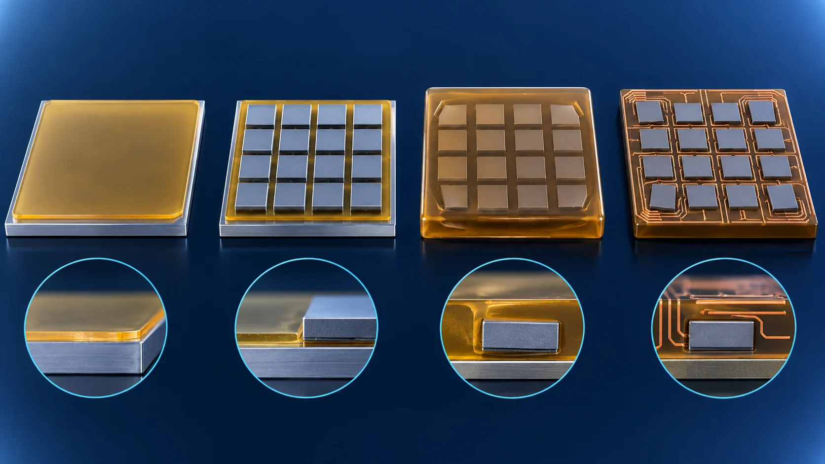
The standard way to build a fan-out package is a sequence called mold first.
- Coat a carrier plate with temporary adhesive
- Place the singulated dies onto it in precisely the right positions
- Encapsulate the whole thing in resin (mold)
- Release the carrier and build the redistribution layer (RDL) on the molded face
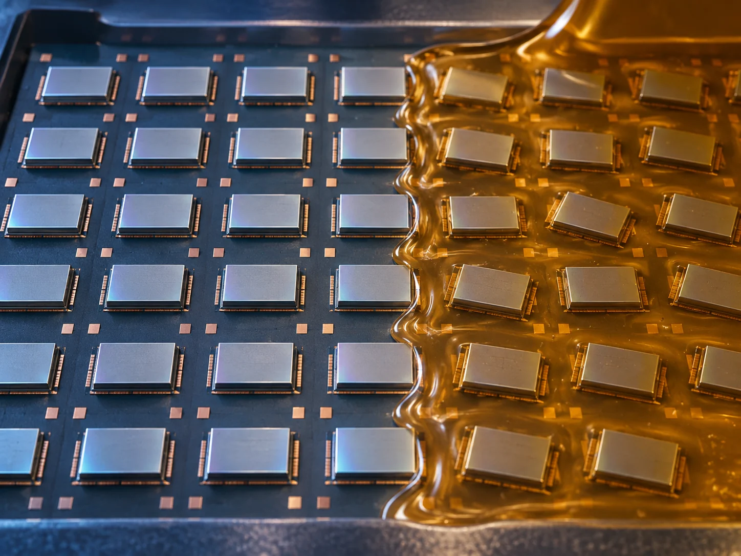
Step 3 is the problem. Molding compound shrinks as it cures, and expands and contracts with temperature. That flow and shrinkage push the dies, and the positions so carefully set in step 2 drift slightly. That is die shift.
5. A materials engineer's view: the combination decides the result
imec has published results from tackling die shift and warpage head-on.
The imec demonstration quoted below was carried out as fan-out on a 300 mm wafer (FO-WLP)Sourced. These are not panel results. That said, die shift and warpage are already the central issues at wafer level, and moving to a panel makes them harder still. Read this as a reference point for the accuracy the field has reached.
The published numbers
| Item | As published |
|---|---|
| Placement accuracy target | Within 3 µm between die and carrier |
| Achieved | Die-to-carrier shift below 2 µm, even after 2 hours at 200 degrees C |
| Warpage | Below 200 µm across a full 300 mm wafer |
| Assessment | These values are described as well below those reported in the literature |
| Bump pitch | 40 µm and 20 µm |
| Package thickness | 300 to 400 µm (excluding solder balls) |
All rows Sourced (imec magazine, April 2020). The work received the 2019 3D InCites Process of the Year award.
What was actually combined
The striking thing is that imec solved this not with a single material or tool, but by optimising a combination.
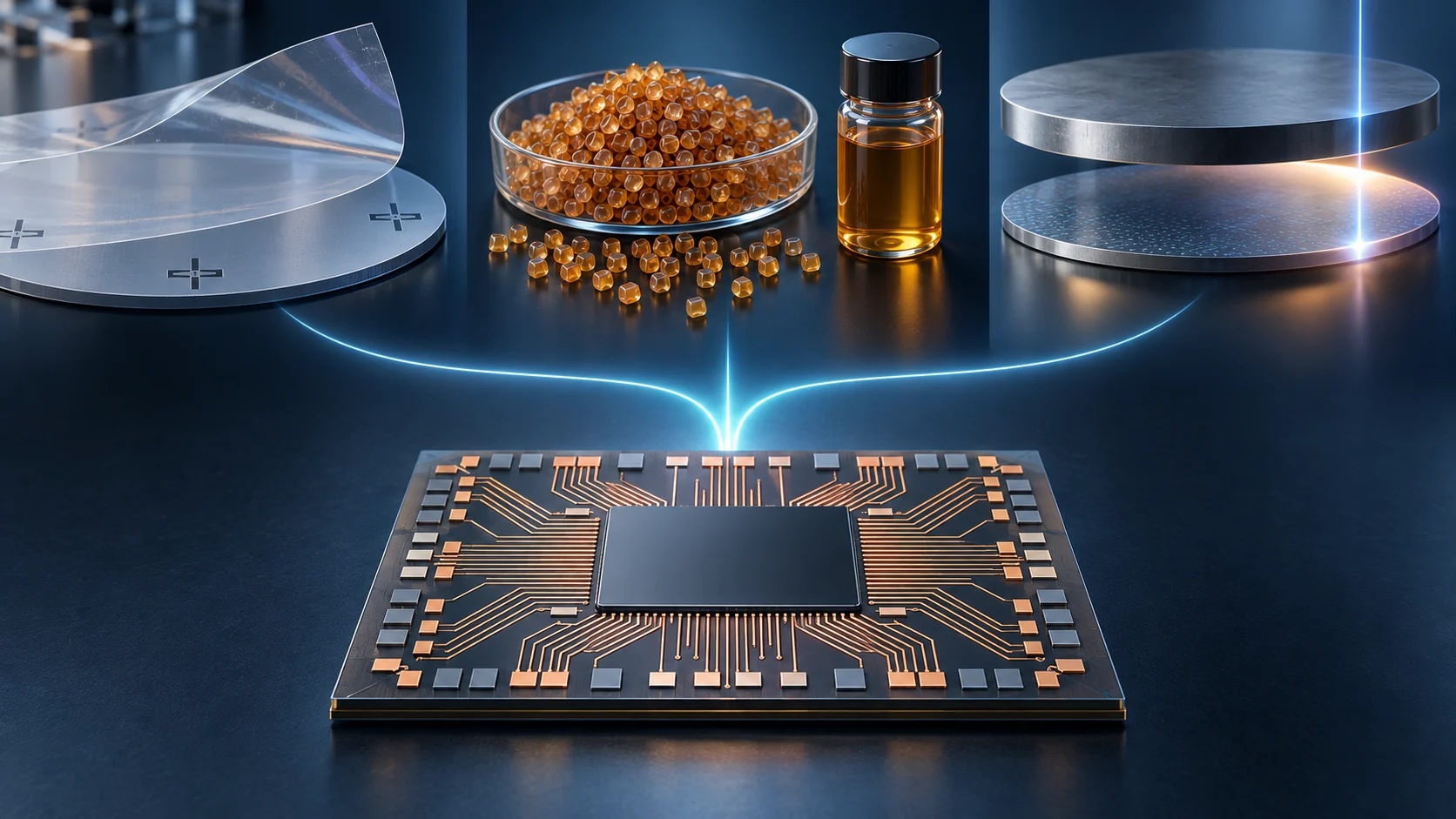
"The temporary adhesive has to be transparent." That single requirement tells you a lot about the nature of the constraint. An adhesive is normally asked to stick, to release, and to survive heat. Here it also has to be optically clear enough to read the alignment marks underneath it. The adhesive is being judged as an optical component too.
"Granular is more stable than liquid, because its glass transition temperature is higher." That is equally telling. Even within the same chemistry, the supply form changes the thermal properties, and that feeds straight through to die placement accuracy — an outcome that looks entirely unrelated.
It also matters that the two carriers are released differently (mechanically, then laser-assisted). Even for the same function of "stick temporarily, then release", the best answer changes with where in the flow you use it. What makes PLP materials development hard is not the performance of any individual material; it is the number of combinations.
6. Activity in Japan: Resonac's JOINT3
On 3 September 2025 Resonac announced the launch of JOINT3, a consortium of 27 companiesSourced (Resonac).
| Item | As announced |
|---|---|
| Participants | 27 companies |
| Structure | Led by Resonac, with 26 partner companies in Japan, the United States, Singapore and elsewhere |
| Focus | Process development for panel-level organic interposers (510 x 515 mm) |
| Aim | Accelerating development of materials, equipment and design tools through co-creation with the partners |
| Application | 2.xD packages for AI chips and HBM, placing several dies side by side |
| Sites | APLIC (Shimodate works, Yuki, Ibaraki) and the Packaging Solution Center (Kawasaki) |
| Timing | Pilot line scheduled to run in 2026 |
All rows Sourced (Resonac announcement, 3 September 2025). The company frames the programme as a response to the industry-wide move from round wafers to rectangular panels for better production efficiency.
As Section 5 showed, PLP outcomes are decided by combinations of materials. And evaluating a combination requires a line you can actually run it on, and the tools to design it. No single company closes that loop, which is why it takes the form of a consortium — a sign that the era of a materials company selling materials alone is ending.
7. What is still hard
(1) Warpage
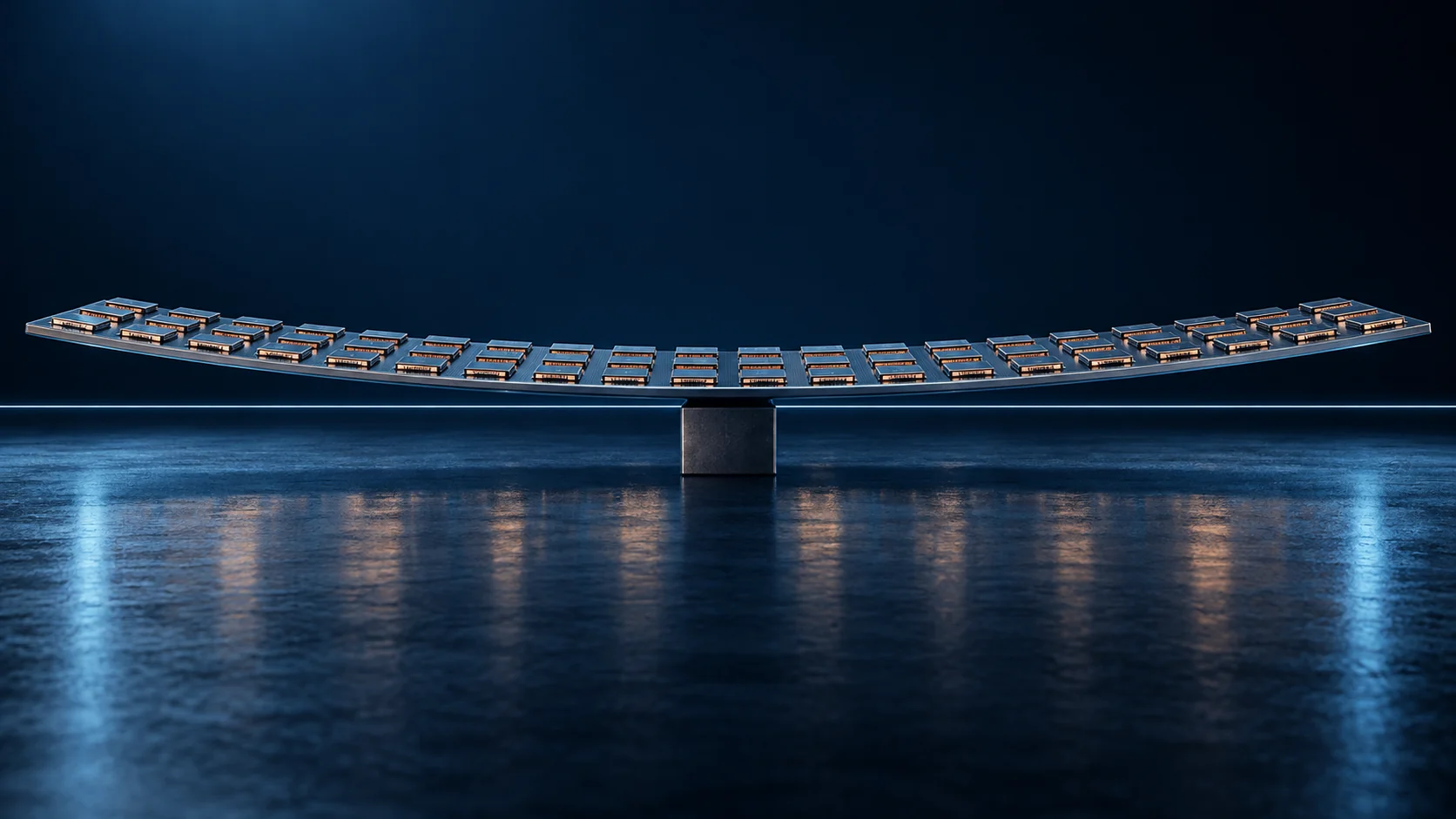
The larger the area, the larger the warpage. SEMI's survey named flatness and warpage, alongside dimensions, as things needing standardisationSourced. Holding flatness across a whole panel feeds directly into lithographic depth of focus and into handling downstream.
(2) Uniformity over a large area
Exposure, plating, deposition — every one of them has to hold the same conditions across the whole panel. If film thickness or line width differs between centre and edge, the parts at the edge are the ones that fail.
(3) The weight of a single sheet
Building 100 units on one panel also means that one bad panel loses 100 units. More units per sheet is also more risk per sheet.
(4) The equipment does not yet exist
Tools built for round wafers cannot simply be reused. Transport, chucking, and any step that assumes rotation — spin coating, for example — may not work on a large rectangle. That is exactly why SEMI 3D20 standardised the dimensions: to let an equipment industry form around them.
8. Glossary
- PLP
- Panel Level Packaging. Building packages on a large rectangular panel.
- FOPLP
- Fan-Out Panel Level Packaging. Fan-out packages built on a panel.
- FOWLP
- Fan-Out Wafer Level Packaging. The same thing built on a wafer.
- Mold first
- Placing the dies, encapsulating them, and only then building the redistribution layer.
- Die shift
- Placed dies drifting out of position because of flow and shrinkage during molding.
- Carrier
- A temporary plate that supports dies or a panel during processing.
- Temporary bond material (TBM)
- The material used to attach to a carrier, removed once the steps are done.
- Debonding
- Releasing the carrier. Done mechanically or with a laser.
- Molding compound
- The resin that encapsulates the dies. Supplied as a liquid or as granules.
- Glass transition temperature (Tg)
- The temperature at which a resin changes from rigid to soft.
- Edge exclusion
- The outer region of a wafer or panel where quality is not guaranteed and no product is built.
- SEMI 3D20
- The SEMI standard specifying panel dimensions, thickness, warpage and mass for PLP.
- SEMI M1
- The specification for polished monocrystalline silicon wafers, referenced by 3D20.
- Organic interposer
- An interposer built from organic materials rather than silicon.
- 2.xD package
- A general term for assemblies that place several dies side by side.
9. Primary sources
- SEMI "Standard for Fan-Out Panel Size Ready to Ballot", 28 August 2018 — semi.org
- SEMI "SEMI 3D20 - Specification for Panel Characteristics for Panel Level Packaging (PLP) Applications" — store-us.semi.org
- imec "Temporary bonding and mold process to enable next-gen fan-out wafer-level packaging", imec magazine, April 2020 — imec-int.com
- Resonac "Launch of JOINT3, a consortium with 27 participating companies" (Japanese-language release), 3 September 2025 — resonac.com
- Nippon Electric Glass "Development of GC Core, a glass-ceramic core substrate in a large 515 x 510 mm panel size" (Japanese-language release), 15 January 2025 — neg.co.jp
10. Claim-to-source audit
| Claim in the text | Basis | Label |
|---|---|---|
| Units per sheet: 93 versus 400 at 25 mm square, 21 versus 100 at 50 mm square, 7 versus 36 at 75 mm square. Wafer area utilisation of 82%, 74% and 56%. An area ratio of 3.72x | Our calculation for a 300 mm wafer (pi times 150 squared) and a 510 x 515 mm panel, using grid placement, requiring all four corners inside the wafer, and optimising the placement offset. Edge exclusion is not modelled, so real wafer counts would be lower | Our calculation |
| Processes had been developed for more than ten panel sizes; the parallel with the proliferation of wafer sizes in the 1970s; more than 70% support and under 2% opposition to standardisation; edge profile, flatness and warpage named as items to standardise | SEMI blog, 28 August 2018[Source 1] https://www.semi.org/en/blogs/semi-news/standard-for-fan-out-panel-size-ready-to-ballot | Sourced |
| SEMI 3D20 specifies panel outline dimensions, thickness, warpage and mass for PLP. First edition 3D20-0719 (July 2019), current edition 3D20-0921 (September 2021). It references SEMI M1. The scope states that many sizes slow adoption and force equipment customisation | SEMI 3D20 standard listing[Source 2] https://store-us.semi.org/products/3d02000-semi-3d20-en-specification-for-panel-characteristics-for-panel-level-packaging-plp-applications | Sourced |
| imec: placement accuracy target within 3 µm; die-to-carrier shift below 2 µm even after 2 hours at 200 degrees C; warpage below 200 µm across a full 300 mm wafer; values well below those reported in the literature; bump pitches of 40 µm and 20 µm; package thickness 300 to 400 µm; 2019 3D InCites Process of the Year | imec magazine, April 2020[Source 3] https://www.imec-int.com/en/imec-magazine/imec-magazine-april-2020/temporary-bonding-and-mold-process-to-enable-next-gen-fan-out-wafer-level-packaging | Sourced |
| imec: BrewerBOND C1301 for room-temperature die bonding, transparent enough for alignment mark recognition; liquid and granular molding compounds compared, with granular more stable against temperature because of its higher glass transition temperature; first carrier is silicon with alignment marks released mechanically, second uses laser-assisted debonding for throughput | imec magazine, April 2020[Source 3] https://www.imec-int.com/en/imec-magazine/imec-magazine-april-2020/temporary-bonding-and-mold-process-to-enable-next-gen-fan-out-wafer-level-packaging | Sourced |
| That the imec demonstration was fan-out on a 300 mm wafer and not a panel result | imec magazine, April 2020, stated in the text and in a note by this article[Source 3] https://www.imec-int.com/en/imec-magazine/imec-magazine-april-2020/temporary-bonding-and-mold-process-to-enable-next-gen-fan-out-wafer-level-packaging | Sourced |
| Resonac JOINT3: 27 companies, panel-level organic interposers at 510 x 515 mm, co-creation across materials, equipment and design tools, 2.xD packages, APLIC in Yuki (Ibaraki) and Kawasaki, pilot line scheduled for 2026 | Resonac news release, 3 September 2025[Source 4] https://www.resonac.com/news/2025/09/03/3599.html | Sourced |
| The Nippon Electric Glass glass core substrate is 515 x 510 mm | Nippon Electric Glass news release, 15 January 2025[Source 5] https://www.neg.co.jp/news/20250115.html | Sourced |
| That resin shrinkage moves the dies, that the shift scales with distance from centre, that warpage grows with area, and that one failed sheet loses many units | Commentary based on general relationships in materials engineering and manufacturing. No numerical claim is made about any specific product | Commentary |
Last updated 20 September 2026. Sources are limited to primary material (official announcements and standards information from standards bodies, research institutes and manufacturers). All figures are explanatory concept graphics. Visual-overview figures are shown as AI-generated conceptual images, matching the Japanese edition. Vector drawings are retained where they carry quantitative values or precision-critical technical labels. AI-generated images do not depict real equipment, products, facilities, dimensions or exact cross-sections; replaced source SVG overview drawings remain in the HTML but are hidden.