TECHNOLOGY EXPLAINER
What an RDL Is
— the few-micron wiring layer that gives a chip's pads a new address
RDL turns up in every article about advanced packaging and is almost never explained. What it actually is: a wiring layer a few micrometres thick, built straight onto the chip using semiconductor process steps. It is also a field in which Japanese materials makers sit at the centre.
- What an RDL is (the short version)
- Why it exists — giving the pads a new address
- The decisive difference from a package substrate
- Where it is used
- How it is made
- A materials engineer's view: photosensitive polyimide and PBO
- How fine can it go
- When being soft becomes the function — the RDL interposer
- What is still hard
- Glossary / Primary sources / Claim-to-source audit
Sourced = a value stated in published material from a research institute or manufacturer (link given)
Our calculation = a figure this article derived, with the assumptions spelled out
Not yet confirmed = research-stage work with no confirmed production record
1. What an RDL is (the short version)
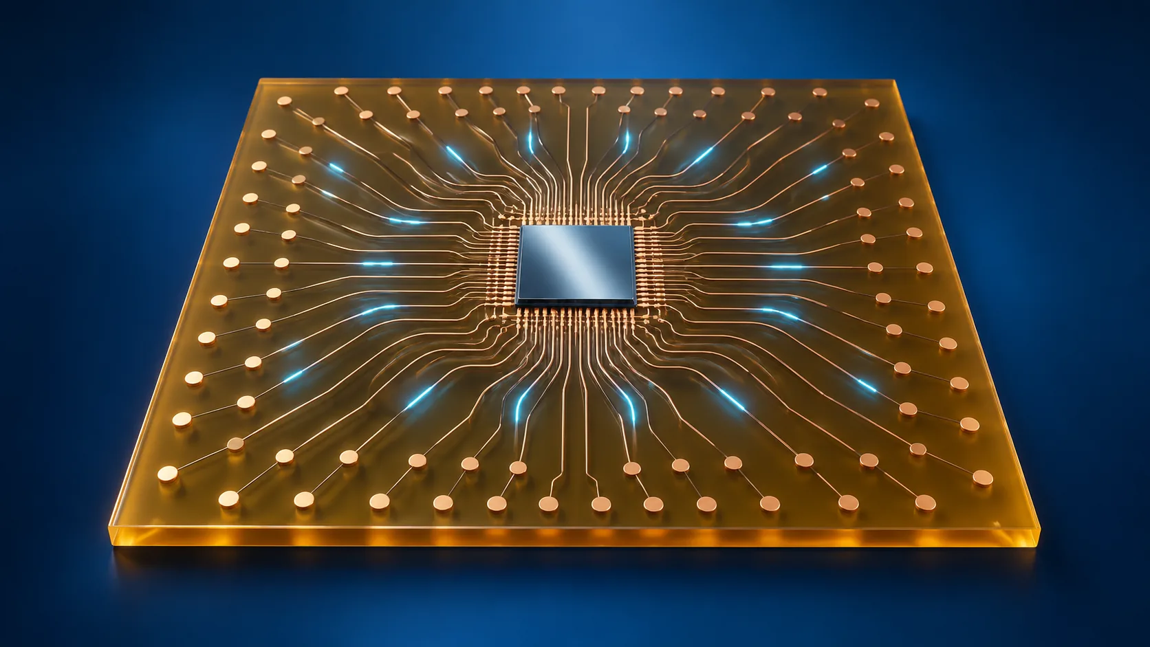
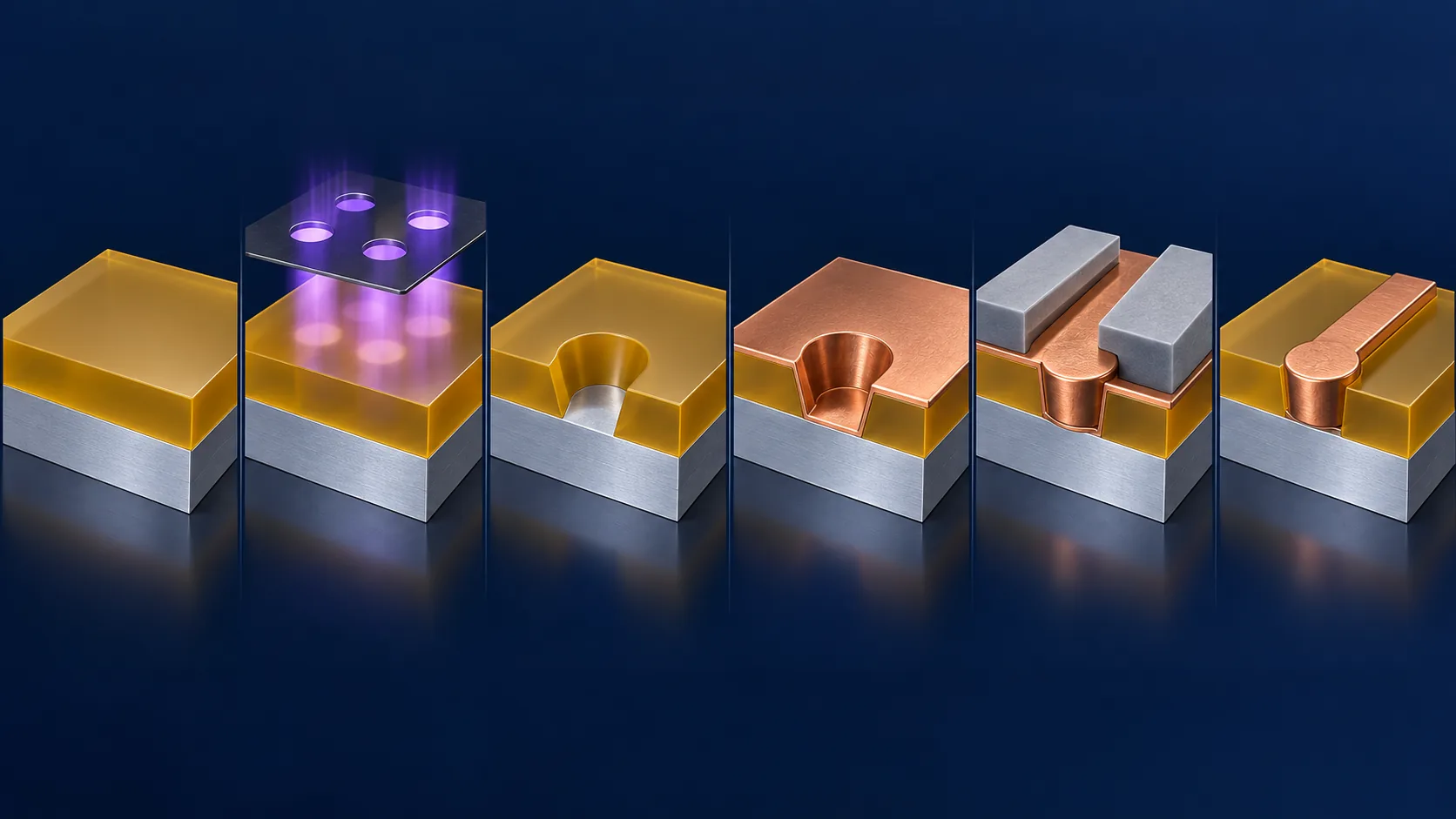
An RDL — Redistribution Layer — is a wiring layer a few micrometres thick, built directly onto the surface of a chip using the same process steps as the chip itself. The name says what it does: it re-distributes the arrangement of the terminals.
- Where it is built: not as a separate component, but directly on the wafer or the panel
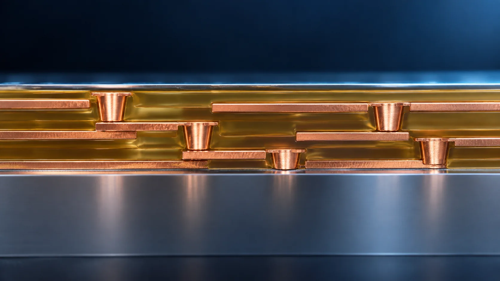
- How it is built: photolithography, sputtering, plating — semiconductor process steps, not printed-circuit-board ones
- What it is for: moving the chip's fine, fixed pads to positions and pitches the outside world can handle
The Package Substrate article described the substrate as a translator between nanometres and millimetres. The RDL does the first stage of that translation not on the substrate but on top of the chip. Part of the translation job has crept off the substrate and onto the silicon side — that is the easiest way to place it.
2. Why it exists — giving the pads a new address
The terminals of a silicon chip — its pads — have a position and a pitch fixed by the chip design. Usually they sit around the edge of the die at an extremely tight pitch.
The outside world cannot receive them like that. A substrate can only handle a much coarser pitch. And in many cases the area of the die itself is simply not big enough to hold all the terminals that are needed.
So you add one more wiring layer on top of the chip and lead the terminals out to wherever you want them. That is an RDL. Spreading terminals out past the outline of the die is what the industry calls fan-out.
3. The decisive difference from a package substrate
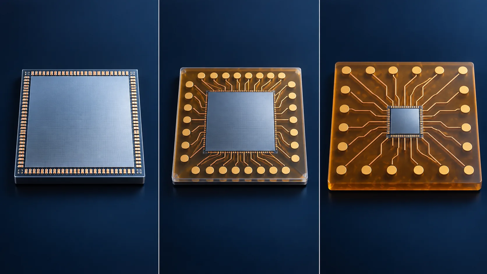
An RDL and a package substrate are both "layers that route wiring around", which is why the two get confused. But they are made in completely different ways.
| RDL (redistribution layer) | Package substrate | |
|---|---|---|
| Where it is built | directly on a wafer or a panel | as a separate board, in its own process |
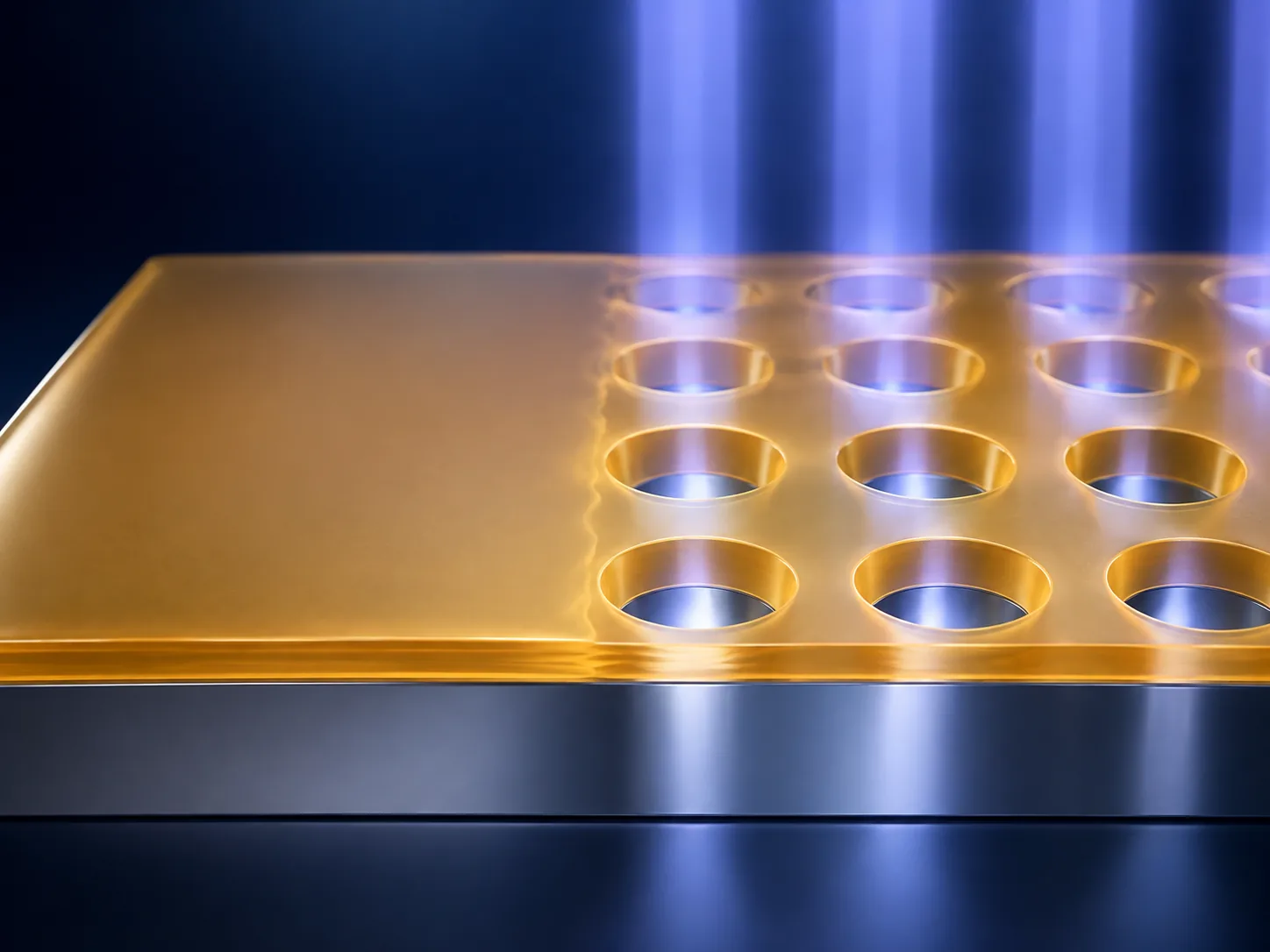
| How holes are opened | exposure and development (the material itself is photosensitive) | laser drilling |
| How traces are formed | sputtered seed layer, then electrolytic copper plating | electroless plating, then electrolytic copper (SAP) |
| Dielectric material | photosensitive polyimide, PBO precursor and the like | build-up film such as ABF |
| Equipment used | front-end semiconductor tools (steppers, sputter systems) | printed-circuit-board tools |
| Line width reached | µm and into sub-µm | tens of µm (UHDI is aiming at single-digit µm) |
In the build-up layers of a substrate, a laser opens the holes. The material is the thing being drilled.
In an RDL, the material is photosensitive and opens holes in itself, through exposure and development.
So an RDL dielectric carries a double role: it is an insulating film and a photoresist at the same time. It has to meet the insulation, mechanical and thermal specifications and still resolve fine features. That is what makes RDL materials hard to develop, and what keeps newcomers out.
4. Where it is used
Fan-out packages
TSMC describes InFO (Integrated Fan-Out) as a wafer-level system integration technology featuring high-density RDL and TIV (Through-InFO Via)Sourced (TSMC).
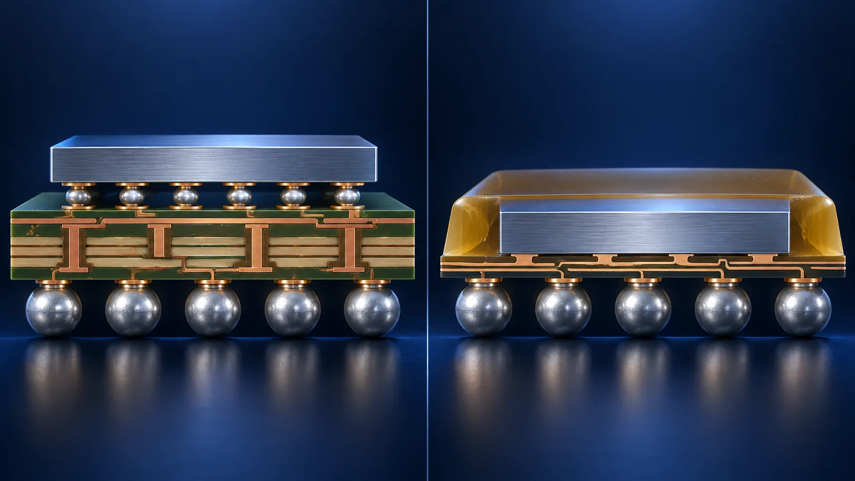
The line worth pausing on concerns InFO-PoP, the industry's first 3D wafer-level fan-out package, which TSMC says "has no organic substrate and no C4 bump, and therefore has better electrical and thermal performance than flip-chip PoP, and is thinner"Sourced.
RDL interposers
The other major use is building the interposer itself out of RDL. TSMC describes CoWoS-R as using an RDL interposer as the interconnect between the SoC and HBM, in volume production since 2023Sourced (TSMC). Section 8 goes into this in detail.
5. How it is made
6. A materials engineer's view: photosensitive polyimide and PBO
This is the heart of the article. RDL dielectrics are mostly photosensitive polyimide and photosensitive PBO (polybenzoxazole) precursors, and Japanese materials makers sit at the centre of this field.
Reading it off a real datasheet
HD8820 from HD MicroSystems is an alkaline-developable positive-tone photosensitive PBO precursor used for redistribution layers and stress buffers. Its published properties are as followsSourced (HD MicroSystems).
| Property | Published value | Why it matters |
|---|---|---|
| Type | alkaline-developable positive-tone photosensitive PBO precursor | compatible with TMAH development |
| Cure temperature | 280 to 350 °C | it is baked on top of a finished device, so lower is better |
| Water absorption | 0.5% | absorbed moisture lowers insulation and causes blistering at reflow |
| Elongation at break | over 100% | essential if the film is to absorb stress and let it go |
| Tensile strength | 170 MPa | the strength of the film itself |
| Modulus | 2.2 to 2.7 GPa | too stiff and it passes the stress straight through |
| Glass transition temperature | 300 °C | it has to survive the heat of later assembly steps |
| 5% weight-loss temperature | 470 to 500 °C | the onset of thermal decomposition |
All values Sourced (HD MicroSystems product page).
For a dielectric material that is a very large number. It points to a design philosophy quite different from the epoxy-based build-up materials used elsewhere in the same package.
The reason is that the RDL doubles as a stress buffer. It sits in direct contact with the silicon die, and silicon expands with heat very differently from the moulding compound and solder outside it. If the stress from that mismatch reached the die unchecked, it would crack the silicon or damage the wiring.
What is being asked of an RDL polymer is not hardness and toughness but the ability to stretch and let the stress go. Tensile strength of 170 MPa for "strength", elongation above 100% for "give", and a modulus of 2.2 to 2.7 GPa for "not too stiff" — specifying all three at once is what that philosophy looks like on a datasheet.
The thermal budget constraint
An RDL is built on top of a finished device. Push the cure temperature too high and you damage the circuitry and wiring underneath. Being able to cure at low temperature is therefore a value in its own right.
JSR says it has developed low-temperature-cure polyimide that can be developed in alkaline solution as a photosensitive dielectric for redistribution layers in WL-CSP and SiP and for fan-out packages, and describes it as low in process cost and low in environmental loadSourced. The company also lists products free of PFASSourced (JSR).
How far back this goes
Sumitomo Bakelite says it began volume production of the world's first positive-tone photosensitive semiconductor wafer coating resin in 1997Sourced. For WLP redistribution use it lists high resolution, strong adhesion to UBM, low water absorption (0.9%) and solvent resistance as features, and gives the roles as protecting the chip from contamination and moisture, improving adhesion to the moulding compound, and preventing filler attack from itSourced (Sumitomo Bakelite).
Moulding compound is loaded with inorganic filler to bring its thermal expansion down. Those hard particles, striking the die surface or the wiring directly, are a source of damage. The RDL polymer works as a physical shield against them as well.
Electrical redistribution, stress buffering, moisture barrier, protection from filler — one layer doing four jobs.
7. How fine can it go
On 2 March 2026 the European NanoIC pilot line led by imec released a PDK (process design kit) for fine-pitch RDLSourced. The published specifications are as follows (imec).
| Item | Published value |
|---|---|
| Line width and space | down to 1.3 µm |
| Microbump pitch | down to 20 µm |
| Dielectric | polymer-based |
| Benefit (UCIe-Advanced die-to-die interface) | up to 40% higher communication speed and up to 15% lower energy per bit |
| Positioning | described as going beyond what leading commercial foundries currently offer |
All values Sourced (imec announcement, 2 March 2026). These are pilot-line results and do not represent a production-level specification.
The package substrate covered in the previous article is aiming, as UHDI, at single-digit-µm line and space. The RDL is already within reach of 1.3 µm. Fineness is the RDL's job; strength and reach as a board are the substrate's — the division of labour shows up plainly in the numbers.
8. When being soft becomes the function — the RDL interposer
For a materials engineer this may be the most interesting section of the article.
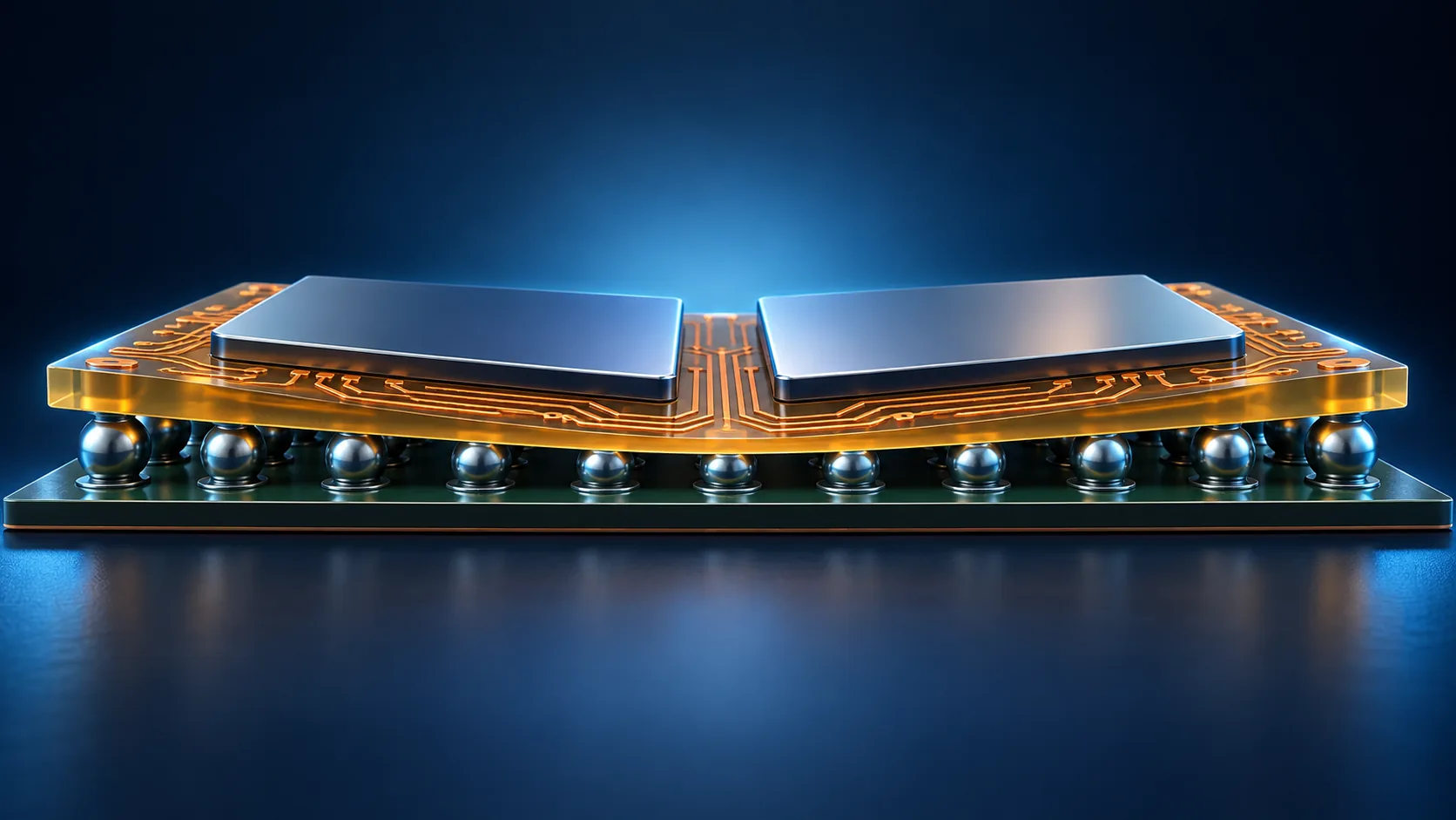
TSMC describes CoWoS-R this waySourced: the RDL interposer consists of polymer and copper traces and is relatively flexible, which enhances C4 joint integrity and allows the package to be made larger for extremely complicated functional requirements (TSMC).
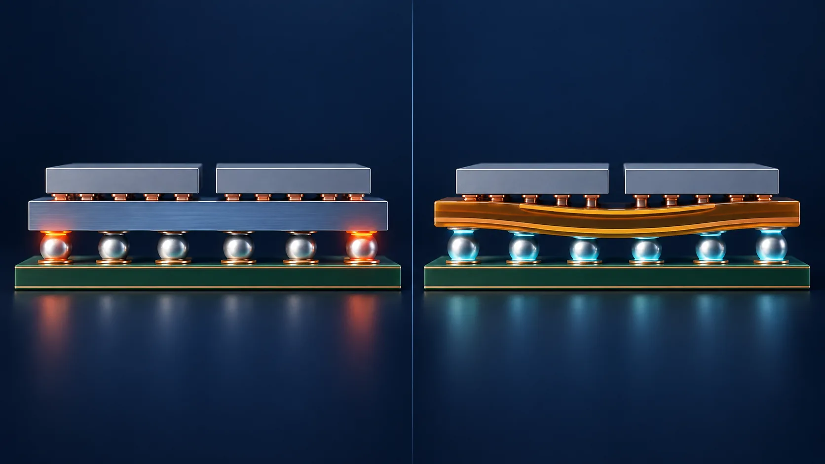
A silicon interposer gives the finest wiring, but it is stiff, brittle, prone to cracking and expensive per unit area. An RDL interposer cannot match it for fineness, yet its compliance — a material property — becomes the reliability argument.
TSMC states that CoWoS-S, which uses a silicon interposer, goes up to 3.3 reticle sizes (around 2,700 mm²), and recommends CoWoS-L or CoWoS-R above thatSourced. What sets the ceiling on package size is not an electrical property but a mechanical one — a clear case of material properties defining directly what assembly can and cannot do.
9. What is still hard
(1) Thermal budget and lower cure temperatures
Because the layer is built on a finished device, you want the cure temperature down. But a film cured at low temperature is generally worse in heat resistance and mechanical properties. Getting a low cure temperature and good film properties at the same time is the central problem of this materials field.
(2) Resolution against film thickness
Finer wiring favours a thin film, but doing the stress-buffer job needs a certain thickness. Resolution and buffering pull against each other, with film thickness in the middle.
(3) Uniformity over a large area
Moving to panel level means holding film thickness and exposure conditions constant across a large surface. The wider you go from wafer to panel, the harder that becomes.
(4) Keeping up with environmental regulation
As JSR's listing of PFAS-free products shows, regulatory compliance has become a condition of material selectionSourced. It is no longer only performance that is constrained, but the composition itself.
10. Glossary
- RDL
- Redistribution layer. A wiring layer formed on the chip that rearranges the placement of its terminals.
- Fan-in
- A layout that keeps the terminals inside the outline of the die.
- Fan-out
- A layout that carries terminals out into the area widened by moulding compound, allowing more of them.
- WLP
- Wafer level packaging. Building the package while the dies are still in wafer form.
- InFO
- TSMC's fan-out technology, characterised by high-density RDL and TIV.
- TIV
- Through-InFO via. An electrode that passes through the moulding compound to connect top and bottom.
- RDL interposer
- An interposer made of polymer and copper instead of silicon. Used in CoWoS-R.
- C4 bump
- The solder bump that joins a chip to a substrate.
- Photosensitive polyimide
- Polyimide that can be exposed with light and developed. It serves as dielectric and resist at once.
- PBO
- Polybenzoxazole. A resin with good heat resistance and low water uptake. It is coated and exposed as a precursor, then cyclised by heat.
- Stress buffer
- A compliant layer that absorbs the stress from thermal expansion mismatch and protects the die.
- Cure
- The thermal step that turns the coated resin into its final film.
- Seed layer
- A thin metal layer deposited over the whole surface as the starting point for electroplating. Formed by sputtering.
- UBM
- Under bump metallurgy. The metal layer placed beneath a bump.
- Filler attack
- Damage to the chip surface or its wiring caused by the inorganic filler in the moulding compound.
- TMAH
- Tetramethylammonium hydroxide, used as an alkaline developer.
11. Primary sources
- imec "NanoIC opens access to first-ever fine-pitch RDL and D2W hybrid bonding interconnect PDKs", 2 March 2026 — imec-int.com
- TSMC "Integrated Fan-Out (InFO) Wafer Level Packaging" — 3dfabric.tsmc.com
- TSMC "CoWoS®" technology page — 3dfabric.tsmc.com
- HD MicroSystems "HD8820" product page (Japanese-language page) — hdmicrosystems.com
- JSR "Packaging Materials" product information (Japanese-language page) — jsr.co.jp
- Sumitomo Bakelite "Semiconductor Wafer Coating Resin SUMIRESIN EXCEL® CRC" (Japanese-language page) — sumibe.co.jp
- AT&S "Ultra-High-Density Interconnect: The Next Frontier for PCBs and IC Substrates" — ats.net
12. Claim-to-source audit
| Claim in the text | Basis | Label |
|---|---|---|
| InFO is a wafer-level system integration technology featuring high-density RDL and TIV. InFO-PoP is the industry's first 3D wafer-level fan-out package and, having no organic substrate and no C4 bump, has better electrical and thermal performance and is thinner | TSMC InFO technology page[Source 2] https://3dfabric.tsmc.com/english/dedicatedFoundry/technology/InFO.htm | Sourced |
| CoWoS-R uses an RDL interposer as its interconnect and has been in volume production since 2023. The RDL interposer consists of polymer and copper traces, is relatively flexible, enhances C4 joint integrity and enables larger packages | TSMC CoWoS technology page[Source 3] https://3dfabric.tsmc.com/english/dedicatedFoundry/technology/cowos.htm | Sourced |
| CoWoS-S goes up to 3.3 reticle sizes (around 2,700 mm²); above that, CoWoS-L or CoWoS-R is recommended | TSMC CoWoS technology page[Source 3] https://3dfabric.tsmc.com/english/dedicatedFoundry/technology/cowos.htm | Sourced |
| The imec NanoIC fine-pitch RDL PDK: line and space down to 1.3 µm, microbump pitch down to 20 µm, polymer-based dielectric, up to 40% higher speed and up to 15% lower energy per bit on UCIe-Advanced, described as going beyond what leading commercial foundries offer | imec press release, 2 March 2026[Source 1] https://www.imec-int.com/en/press/nanoic-opens-access-first-ever-fine-pitch-rdl-and-d2w-hybrid-bonding-interconnect-pdks | Sourced |
| HD8820: alkaline-developable positive-tone photosensitive PBO precursor, cure 280 to 350 °C, water absorption 0.5%, elongation at break over 100%, tensile strength 170 MPa, modulus 2.2 to 2.7 GPa, Tg 300 °C, 5% weight-loss temperature 470 to 500 °C, used as stress buffer and redistribution layer | HD MicroSystems product page[Source 4] https://www.hdmicrosystems.com/jp/products/hd8820 | Sourced |
| JSR has developed low-temperature-cure polyimide developable in alkaline solution for redistribution layers in WL-CSP and SiP and for fan-out packages, describing it as low in process cost and environmental load, and also lists PFAS-free products | JSR product information[Source 5] https://www.jsr.co.jp/products/imple/ | Sourced |
| Sumitomo Bakelite began volume production of the world's first positive-tone photosensitive semiconductor wafer coating resin in 1997. Features listed are high resolution, strong adhesion to UBM, low water absorption of 0.9% and solvent resistance; roles listed are chip protection, adhesion to the moulding compound and prevention of filler attack | Sumitomo Bakelite product page[Source 6] https://www.sumibe.co.jp/product/it-materials/coating/sumiresin-crc/ | Sourced |
| Package substrates are targeting single-digit-µm line and space as UHDI | AT&S technical article[Source 7] https://ats.net/en/ultra-high-density-interconnect-the-next-frontier-for-pcbs-and-ic-substrates/ | Sourced |
| That an RDL material is dielectric and photoresist at once, that elongation at break is what makes stress buffering work, that low cure temperature tends to fight film properties, and that resolution tends to fight film thickness | Commentary drawing on the published properties and on general relationships in materials engineering. It is not a design guideline for any specific product | Commentary |
Last updated 20 September 2026. Sources are limited to primary material (official announcements and product pages from research institutes, manufacturers and materials suppliers). All figures are explanatory concept graphics. Visual-overview figures are shown as AI-generated conceptual images, matching the Japanese edition. Vector drawings are retained where they carry quantitative values or precision-critical technical labels. AI-generated images do not depict real equipment, products, facilities, dimensions or exact cross-sections; replaced source SVG overview drawings remain in the HTML but are hidden.