TECHNOLOGY EXPLAINER
What a System in Package Is
— not only ICs, but resistors, coils and antennas in one body
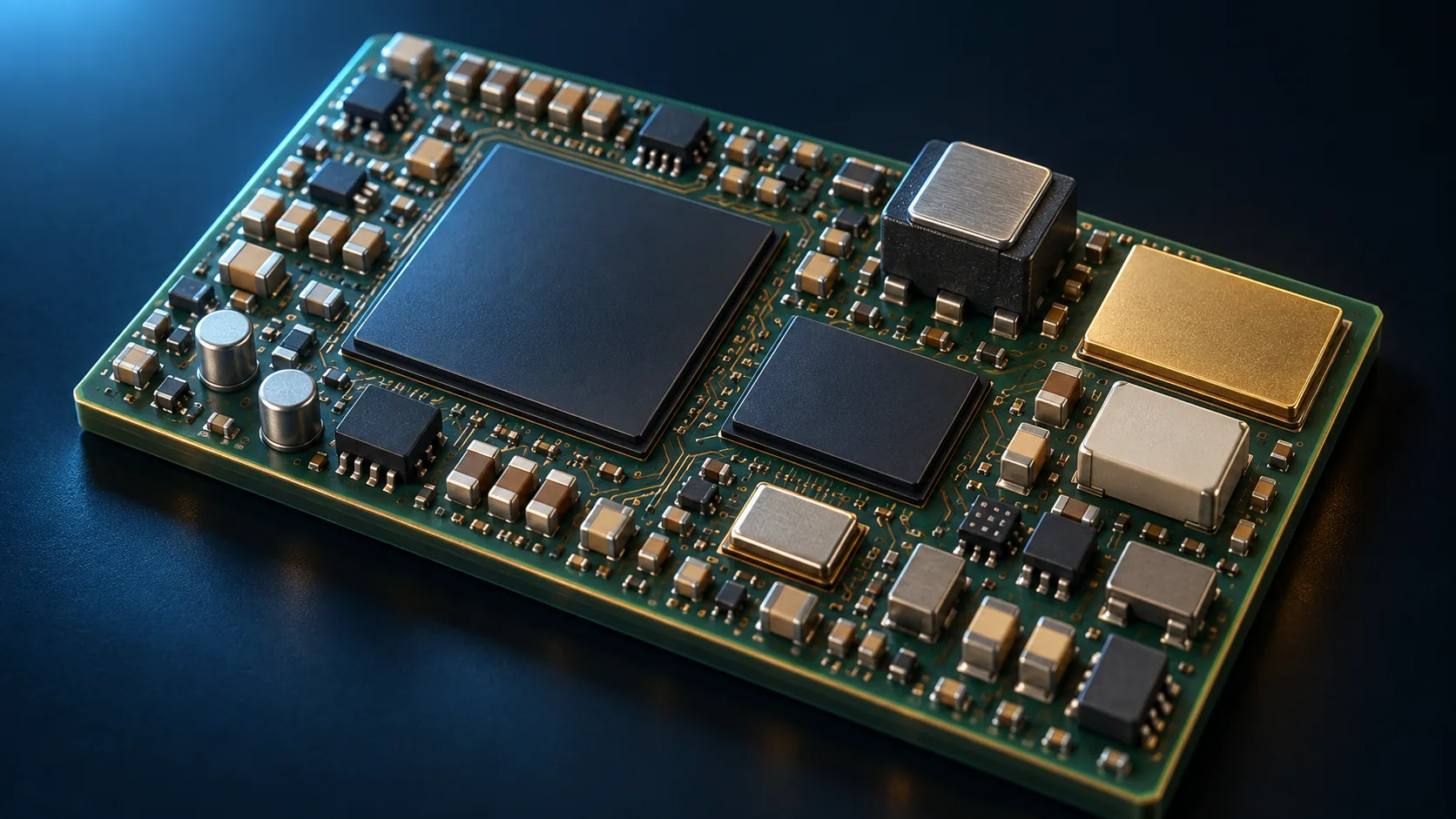
System in Package, usually shortened to SiP. It is an assembly in which everything a system needs in order to work is put inside a single package. And what goes in is not only ICs: capacitors, inductors, filters, antennas, even metal parts. This is the point at which the boundary between semiconductor packaging and electronic-component assembly dissolves.
- What SiP is (the short version)
- How it differs from an SoC — one die, or a collection
- What actually goes inside — not only ICs
- A materials engineer's view (1): use both faces, then bury parts in the board
- A materials engineer's view (2): shielding, the other layer
- What is still hard
- Glossary / Primary sources / Claim-to-source audit
Sourced = a value stated in published material from a research institute or manufacturer (link given)
Our calculation = a figure this article derived, with the assumptions spelled out
Not yet confirmed = research-stage work with no confirmed production record
Anything that is our own structural reading or materials-design interpretation is marked separately as Commentary.
1. What SiP is (the short version)
SiP (System in Package) is an assembly that puts everything needed to make a working system inside one package.
Amkor describes its own SiP offering as "Integration solutions in a package", aimed at "higher levels of integration and lower cost"Sourced. The target is "markets that demand a smaller size with increased functionality"Sourced.
- What goes in: ICs, passives (capacitors, inductors, resistors), filters, antennas, mechanical parts
- Where it is used: RF (the high-frequency front end of a smartphone), wearables, automotive
- What makes it unusual: semiconductor assembly and electronic-component mounting happen inside the same package
Most of the technologies covered in this series have been about how to connect one piece of silicon to another. SiP steps outside that. Things that are not chips start arriving.
Multilayer ceramic capacitors, ferrite inductors, quartz resonators, SAW filters, a metal shield — materials from completely different families now have to live inside one encapsulated body. SiP is the most familiar and by far the most heavily mass-produced form of the idea set out in the Heterogeneous Integration article (Commentary).
2. How it differs from an SoC — one die, or a collection
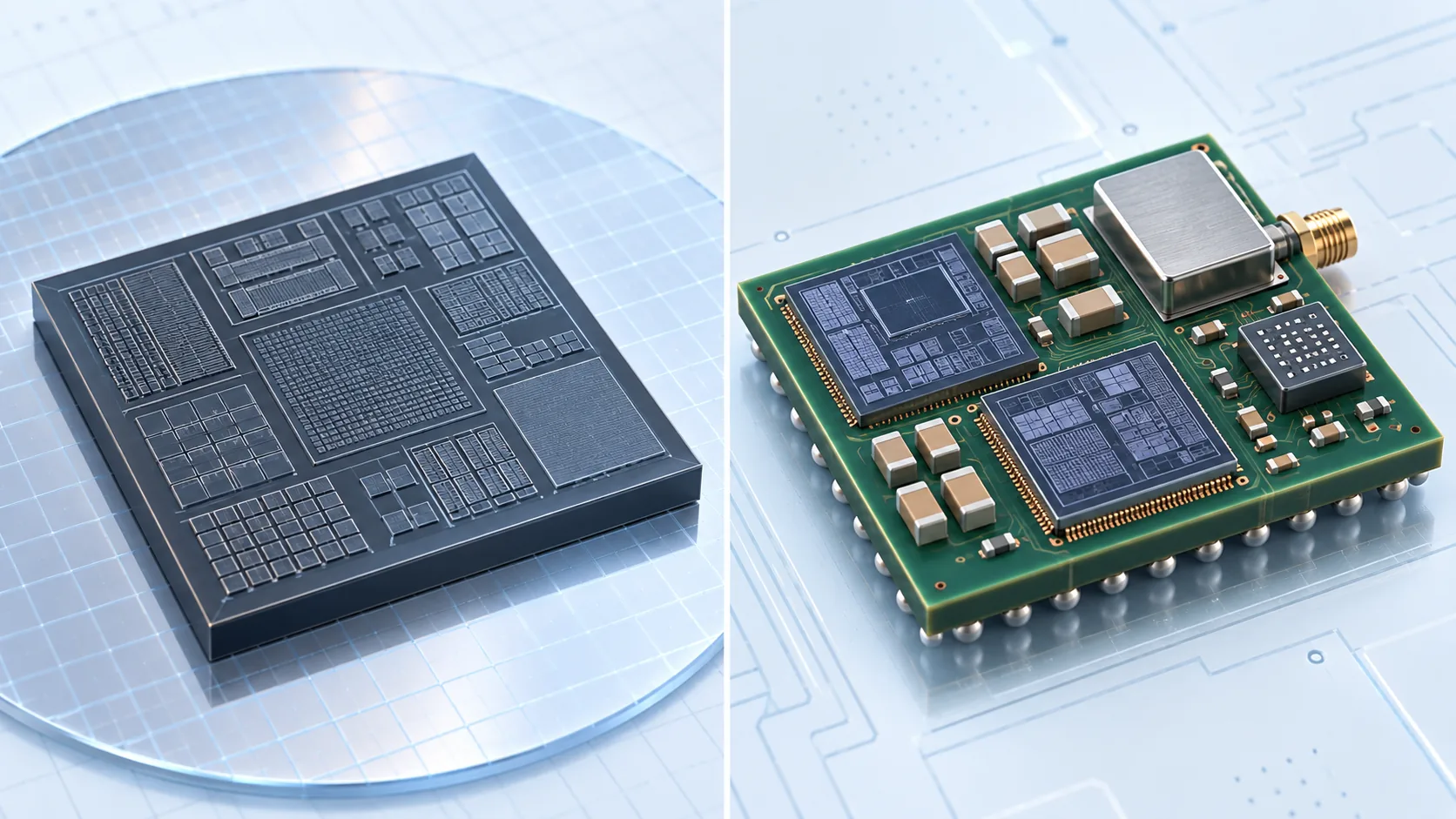
An SoC is powerful, but there are things you cannot build on silicon.
- Large capacitors: the dielectric volume required simply is not available on a die
- High-current inductors: they need magnetic material, which has no place in a silicon process
- RF filters: SAW and BAW rely on piezoelectric material, an entirely different family
- Antennas: their size is set by wavelength, so they cannot be shrunk like a circuit
So the answer is to build each part from whatever material suits it best, then bring them together afterwards. That is the idea behind SiP.
The definition used in the Heterogeneous Integration article was integrating separately manufactured components into a higher-level assembly. SiP is exactly that, with one distinguishing feature: materials other than silicon usually take the leading role (Commentary).
3. What actually goes inside — not only ICs
Amkor spells out what an SiP may contain: "ICs, passive devices (inductors, capacitors, resistors, filters and diplexers), antennas and mechanical parts"Sourced.
In an RF front-end (RFFE) module, "power amplifiers (PA), low-noise amplifiers (LNA), switches, transceivers, filters and discrete antenna" are integrated into a single packageSourced.
Four technologies are named as the means of that integrationSourced.
4. A materials engineer's view (1): use both faces, then bury parts in the board
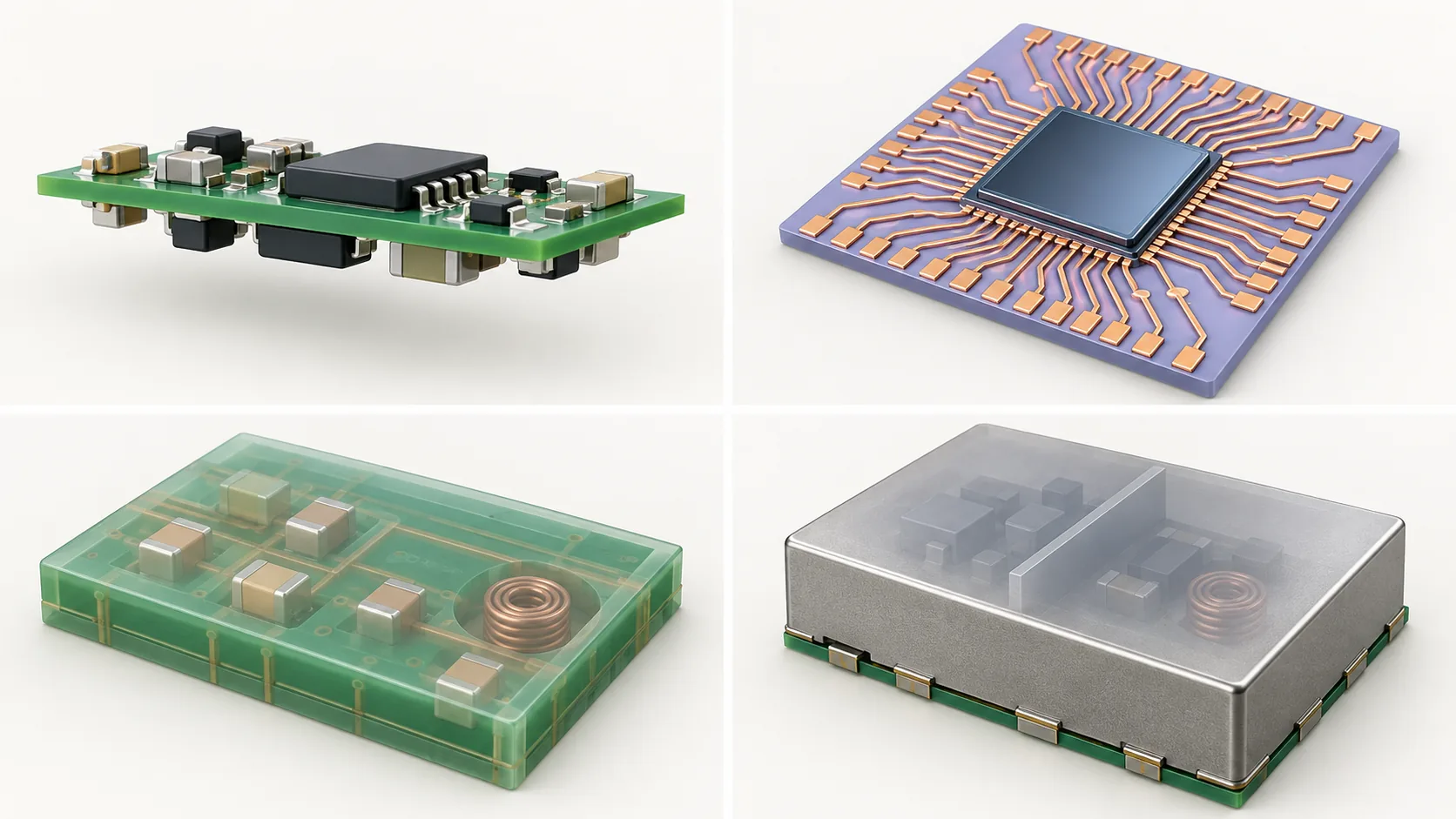
There are broadly two stages to cutting the area of an SiP: use the underside as well, and put parts inside the board.
(1) Use the underside as well
Amkor describes DSMBGA (Double Sided Molded BGA) as a "package which allows molded assembly of components on both sides"Sourced.
Take the same set of components and divide it evenly between the top and the bottomOur calculation.
- Call the mounting area with everything on one face 100
- Split evenly between top and bottom → 50 per face
- In theory the package footprint becomes half
Assumptions: an idealised calculation in which the parts can be divided evenly and there are no routing constraints and no thermal imbalance. In practice the underside imposes height limits, and heat removal and electromagnetic coupling get in the way, so it never works out this cleanly. The package also gets thicker.
The direction is clear enough all the same: if you have run out of plane, use thickness. The same idea that stacked dies in the Stacking article is being applied here to component mounting (Commentary).
(2) Put parts inside the board
Push further and the components can be embedded inside the substrate itself. Murata's iPaS™ is described as a board product with components such as capacitors and inductors embedded and integrated into itSourced.
The company says that embedding SMD components into the board in one go contributes to space saving, lower power consumption and higher functionalitySourced.
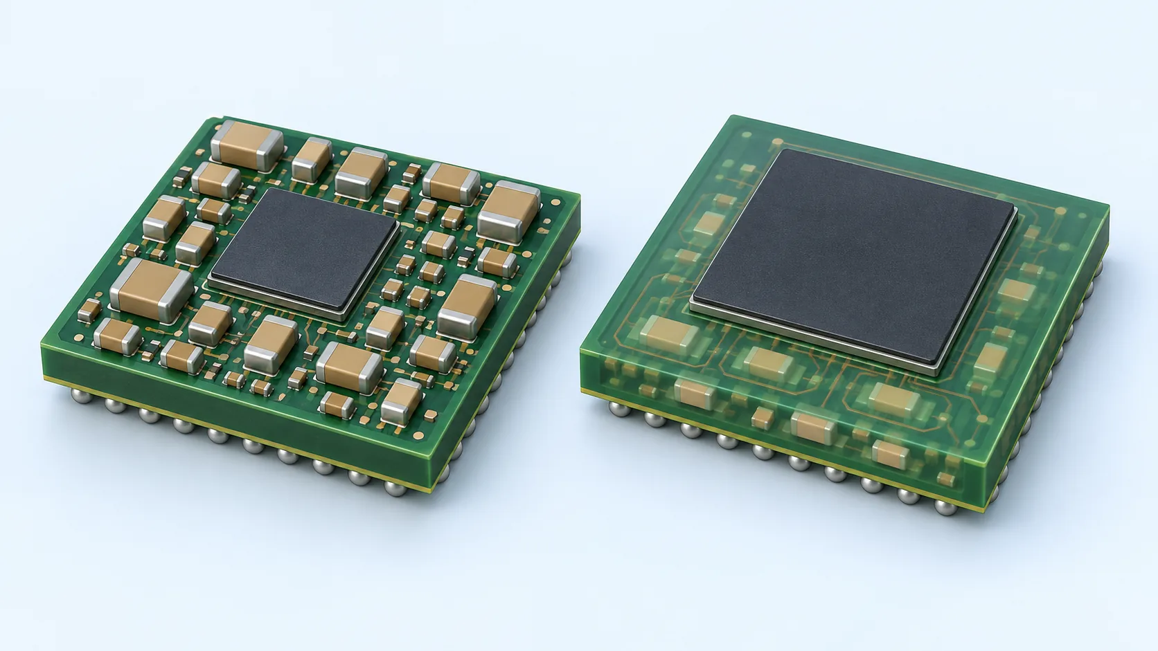
Murata gives three benefits of embedding components in the board: space saving, lower power consumption and higher functionalitySourced. Area is only one of them.
Why lower power? Because the wiring gets shorter. Put a capacitor directly beneath the IC and the power path becomes as short as it can be. It is the board-side version of the idea seen in the Flip Chip article: feed power straight into the middle of the die.
When the same company lists, among the applications for iPaS™, power supply lines for servers and base stations, and vertical power delivery designs for high-performance semiconductor packagesSourced, this is exactly the context. The demand for vertical power delivery seen in the Co-Packaged Optics and Bridge articles is showing up here too, in the form of an embedded-component board — the same problem, answered from a different discipline (Commentary).
Seen from the materials side, embedding is a hard problem.
- Trapping a ceramic part inside a resin board → a CTE mismatch (see the Underfill article)
- Stacking build-up layers on top of it → steps and planarity (the same picture as the Bridge article)
- An embedded part can never be reached again → screening for known good parts beforehand is mandatory
Once you bury something, you cannot get it back out. That problem repeats here as well (Commentary).
5. A materials engineer's view (2): shielding, the other layer
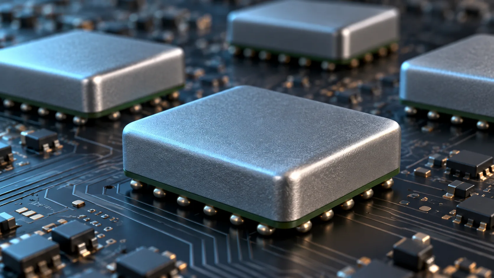
The fourth technology element Amkor names is "sophisticated RF shielding techniques"Sourced.
Inside an SiP, things that radiate (power amplifiers, antennas) sit next to things that are vulnerable to radiation (low-noise amplifiers, sensors). The closer they are, the more they interfere. Hence the metal film around them.
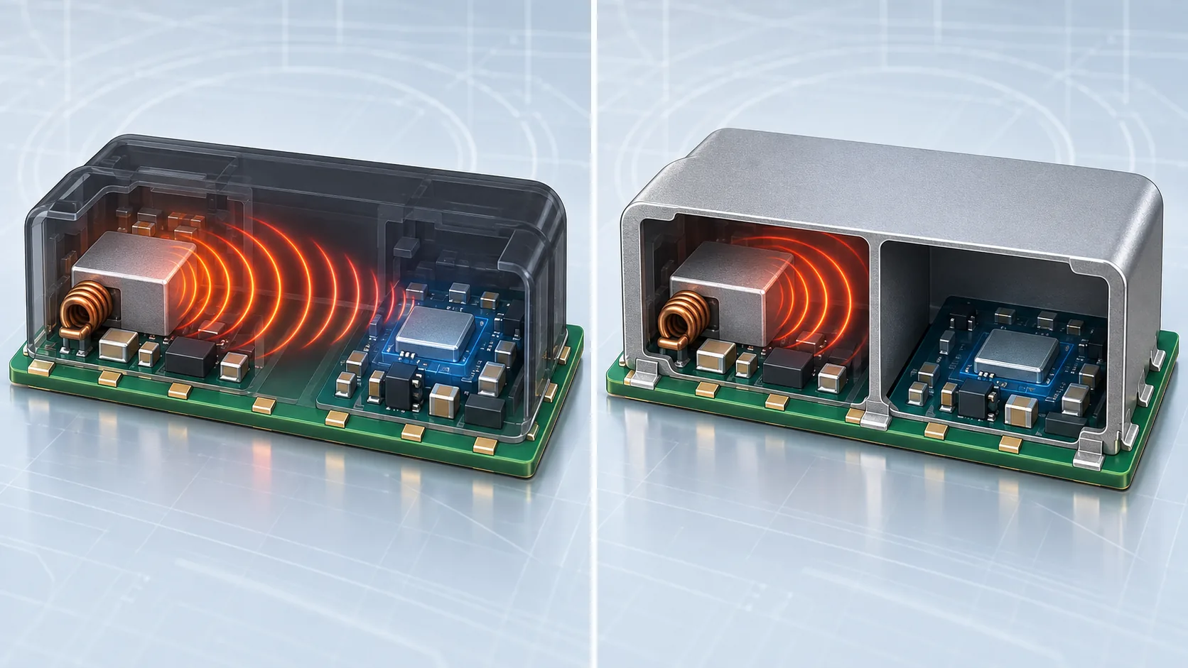
What is interesting here, materially, is that the shield is formed on the outside of the moulding compound.
A conductive film is deposited over the surface of a module that has already been moulded, wrapping around its sides. A further layer goes on after encapsulation is finished.
And what that layer has to deliver belongs to a different family of properties from anything else in this series.
- Conductivity: high enough to reflect or absorb the radiation
- Adhesion: metal on resin (the same problem as desmear in the Via article)
- Step coverage: it must wrap around sidewalls and steps without breaking continuity
- Thinness: a thick film makes the module bigger
Deposit metal thinly and continuously onto resin — put that way, it is the same problem as seed-layer formation in the Via article. Materials work in back-end processing keeps meeting the same problem in different settings (Commentary).
6. What is still hard
(1) The more parts there are, the more the yields multiply
An SiP holds tens to hundreds of components. As the Test and Co-Packaged Optics articles showed, a single bad part makes the whole module bad.
So an SiP takes it as given that every part is known to be good before it is placed. It is the same point ASE makes when it lists "The use of known good die (KGD)" among the advantages of fan-outSourced (Commentary).
(2) Different material families, exposed to the same heat
Silicon, ceramic, resin, metal and piezoelectric material all live together in an SiP, and every one of them has a different coefficient of thermal expansion.
As the Underfill article showed, a CTE mismatch generates stress every time the temperature changes. The more component types there are, the more CTE pairings there are — and that is the core reason reliability design for SiP is so difficult (Commentary).
(3) The demand for miniaturisation never stops
In a technical article on 5G, Murata writes that electronic devices are expected to become still more complex in order to meet consumer expectations for smaller and thinner devices, so that the reliability and the miniaturisation of component technology become essentialSourced.
As a concrete example the company notes that multilayer ceramic capacitors (MLCCs) have shrunk from the 0402 size to the 0201 package, so that a part rated at "2.2uF capacitance, 10V rated voltage" can now be sourced in the smaller packageSourced.
The components themselves get smaller, the mounting gets denser, and then they get buried in the board. Three kinds of miniaturisation are running at once (Commentary).
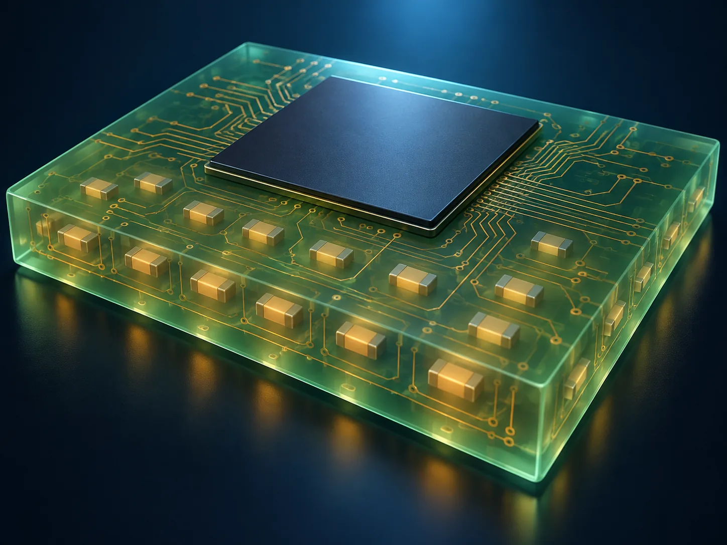
SiP is the article in this series in which things other than semiconductors most clearly take the lead.
- What goes in: ICs, passives, filters, antennas, mechanical parts — material families all over the map
- How they are packed: mounted on both faces, buried in the board, wrapped in a metal film
- What makes it hard: more CTE pairings, yields that multiply out, and buried parts you cannot reach
And the problems that have come up again and again in this series appear here in exactly the same shape: KGD, CTE mismatch, steps and planarity, depositing metal onto resin, and the fact that what you bury stays buried.
The materials change, but the shape of the problems back-end processing faces does not — and SiP shows that more plainly than any other assembly form (Commentary).
7. Glossary
- SiP
- System in Package. An assembly holding everything needed to make a working system inside one package.
- SoC
- System on Chip. All the circuitry built into a single piece of silicon.
- Passive component
- Capacitors, inductors, resistors and the like: parts that neither amplify nor control.
- RFFE
- RF Front End. The high-frequency section of a radio, made up of PAs, LNAs, switches and filters.
- PA / LNA
- Power Amplifier (for transmitting) and Low Noise Amplifier (for receiving).
- Diplexer
- A part that separates signals by frequency band.
- SAW / BAW filter
- High-frequency filters built from piezoelectric material. They cannot be made in silicon.
- AiP / AoP
- Antenna in Package and Antenna on Package: antennas built into or mounted on the package.
- Double-sided mounting
- Placing components on both the top and the bottom of a board.
- DSMBGA
- Double Sided Molded BGA. A package allowing moulded assembly of components on both sides.
- Component-embedded board
- A board with capacitors or inductors buried inside it.
- iPaS™
- Murata's product name for its capacitor- and inductor-embedded boards.
- RF shielding
- Enclosing a region in a conductive film or metal to stop radio interference.
- Conformal shield
- A shielding method in which the conductive film is deposited along the package surface.
- MLCC
- Multilayer ceramic capacitor. The passive component most heavily used in an SiP.
- DC bias characteristic
- How well an inductor keeps its inductance as direct current is passed through it.
- KGD
- Known Good Die: a die guaranteed to be good (covered in detail in the Test article).
- PoP
- Package on Package. Stacking one package on top of another.
8. Primary sources
- Amkor "System in Package (SiP)" — amkor.com
- Amkor "SiP RF" — amkor.com
- Murata "Capacitor / inductor embedded substrate (iPaS™)" (Japanese-language page) — murata.com
- Murata technical article "The challenges of 5G: miniaturisation" (Japanese-language page) — article.murata.com
- ASE "Fan-Out Packaging" (which covers FOSiP) — ase.aseglobal.com
9. Claim-to-source audit
| Claim in the text | Basis | Label |
|---|---|---|
| That Amkor calls SiP "Integration solutions in a package" aimed at "higher levels of integration and lower cost"; that the target is "markets that demand a smaller size with increased functionality"; that SiP, DSMBGA and AiP / AoP are named product categories; that the applications are RF, wearables and automotive compute | Amkor "System in Package (SiP)"[Source 1] https://amkor.com/packaging/system-in-package/ | Sourced |
| That an RFFE module integrates "power amplifiers (PA), low-noise amplifiers (LNA), switches, transceivers, filters and discrete antenna"; that the integration technologies are "double-sided assembly, advanced wafer-level redistribution layers (RDL), passive component integration and sophisticated RF shielding techniques"; that DSMBGA is a "Double Sided Molded BGA (DSMBGA) package which allows molded assembly of components on both sides"; that an SiP may contain "ICs, passive devices (inductors, capacitors, resistors, filters and diplexers), antennas and mechanical parts" | Amkor "SiP RF"[Source 2] https://amkor.com/packaging/system-in-package/sip-rf/ | Sourced |
| That iPaS™ is a board product with components such as capacitors and inductors embedded and integrated into it; that embedding SMD components into the board in one go contributes to space saving, lower power consumption and higher functionality; that it carries electrodes compatible with through-hole and laser-via connection and secures high design freedom through an array structure; that the capacitor type is used for power supply lines in servers and base stations and for vertical power delivery designs for high-performance semiconductor packages; that the inductor type targets high-speed optical transceivers at "400Gb/s, 800Gb/s, 1.6TGb/s"; that the inductor type achieves a DC bias characteristic of 10 A or more and can handle large currents of several tens of amperes | Murata "iPaS™"[Source 3] https://www.murata.com/ja-jp/products/pcb/integrated-package-solution | Sourced |
| That electronic devices are expected to become still more complex in order to meet consumer expectations for smaller and thinner devices, so that the reliability and miniaturisation of component technology become essential; that MLCCs have shrunk from the 0402 size to the 0201 package and that a part rated "2.2uF capacitance, 10V rated voltage" can now be sourced in the smaller package | Murata technical article "The challenges of 5G: miniaturisation"[Source 4] https://article.murata.com/ja-jp/article/5g-miniaturization | Sourced |
| That ASE lists "The use of known good die (KGD)" among the advantages of fan-out; that a product called FOSiP (Fan-Out System in Package) exists | ASE "Fan-Out Packaging"[Source 5] https://ase.aseglobal.com/en/technology/fan_out | Sourced |
| That splitting the same set of components evenly between the two faces halves the package footprint in theory | Our calculation. An idealised case assuming the parts can be divided evenly and that routing, height limits, heat removal and electromagnetic coupling raise no issues. In practice it does not work out this way, and the package gets thicker | Our calculation |
| The list of what is hard to build on silicon (large capacitors, high-current inductors, RF filters, antennas); the SoC-versus-SiP contrast; the explanation that embedding shortens wiring and therefore saves power; the point that burying a ceramic part in a resin board creates CTE mismatch, steps and loss of access; the account of the shield being deposited outside the moulding compound and the properties it demands (conductivity, adhesion, step coverage, thinness); the point that yields multiply as component count rises; the point that more material families mean more CTE pairings; the transmit-to-receive interference explanation and the drawing style of Fig. 5 | Commentary by this article, built on published material. Not a view expressed by any of the companies cited | Commentary |
| That Figs. 1, 2, 4 and 5 are explanatory drawings rather than real observations or engineering drawings | Our note in this article | Commentary |
Last updated 20 September 2026. Sources are limited to primary material (official product pages and technical articles from packaging manufacturers and electronic component manufacturers). Because the text includes our own structural reading and materials-design interpretation, those passages are marked as Commentary and kept distinct from sourced fact. All figures are explanatory concept graphics. Visual-overview figures are shown as AI-generated conceptual images, matching the Japanese edition. Vector drawings are retained where they carry quantitative values or precision-critical technical labels. AI-generated images do not depict real equipment, products, facilities, dimensions or exact cross-sections; replaced source SVG overview drawings remain in the HTML but are hidden.