TECHNOLOGY EXPLAINER
Underfill and Encapsulants
— the resin in the gap is what sets the lifetime
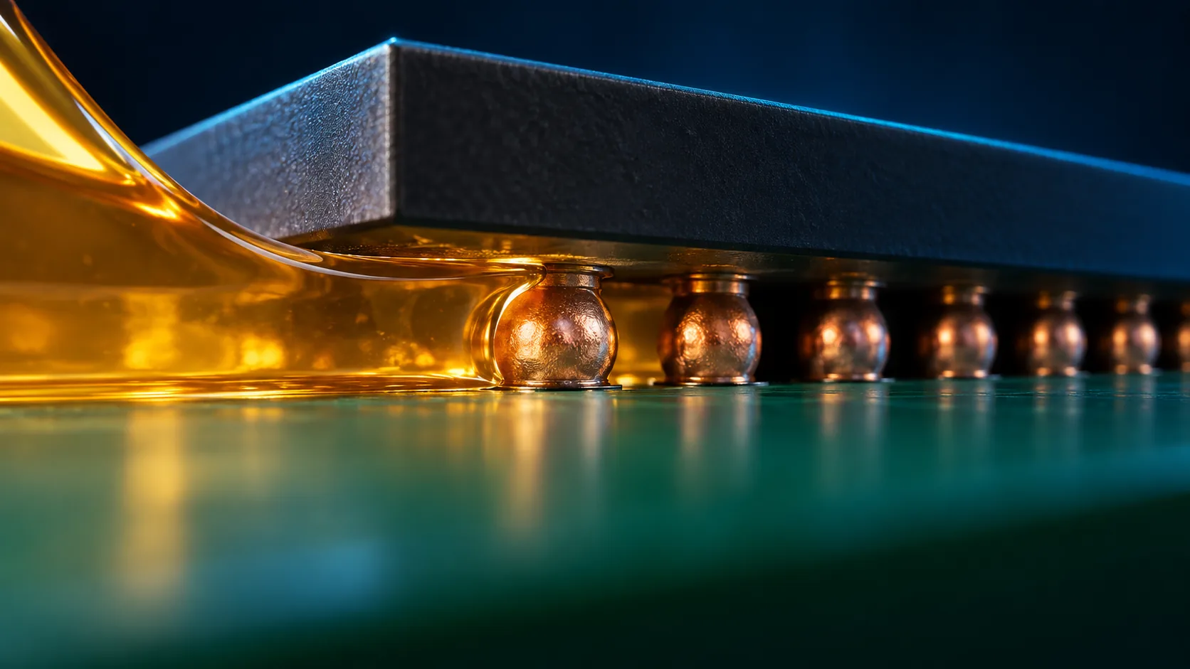
Between a chip and its substrate there is a gap of a few tens of micrometres. Underfill is what fills it; encapsulant is what covers the whole assembly. Both are epoxy resin mixed with silica powder. They look unremarkable, and yet how many temperature swings a package survives is decided by this resin.
- What underfill and encapsulant are (the short version)
- Why the gap has to be filled — the CTE mismatch you cannot escape
- Four ways to fill it
- A materials engineer's view 1: filler particle size sets the gap you can fill
- A materials engineer's view 2: above Tg the material is a different material
- A materials engineer's view 3: the same material, developed both stiffer and softer
- What is still hard
- Glossary / Primary sources / Claim-to-source audit
Sourced = content stated in a company's published material (link given)
Our calculation = a figure this article derived, with the assumptions spelled out
Not yet confirmed = work in development with no confirmed production record
Beyond those, readings about materials design are marked Commentary.
1. What underfill and encapsulant are (the short version)
This article is about two resins used in back-end assembly.
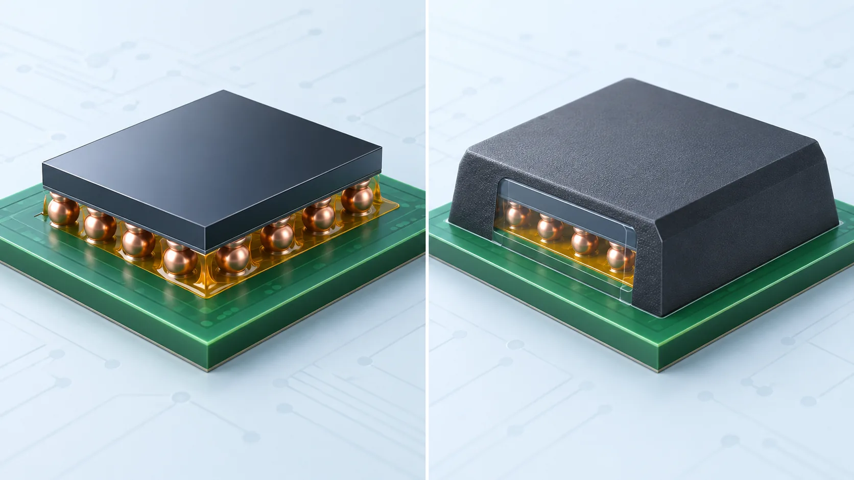
- Underfill: the resin that fills the gap between chip and substrate
- Encapsulant (EMC): the resin that covers the chip and its surroundings entirely
Resonac describes underfill as "a polymer material that seals and reinforces the gap between chip and substrate, relieving the stress on the solder bumps that comes from thermal cycling and the like"Sourced.
For encapsulant, Sumitomo Bakelite lists four roles: "protecting the chip", "providing insulation from the external environment", "providing a path for heat to spread away from the chip" and "providing handleability during mounting"Sourced.
2. Why the gap has to be filled — the CTE mismatch you cannot escape
Why fill the gap at all? Why not leave air in there? You cannot, and the reason is thermal expansion.
Resonac explains that CUF (capillary underfill) is "filled into the gaps between members with large CTE differences: the chip, the interposer and the package substrate", and that it "serves to distribute stress across the whole area, preventing delamination and open circuits"Sourced.
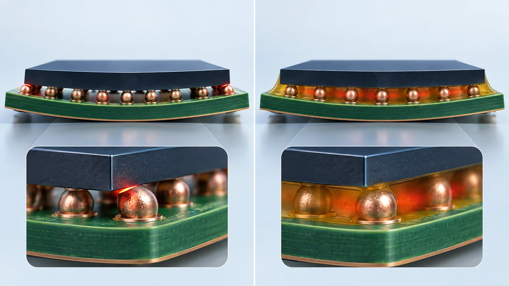
Think of underfill as "glue that fills a gap" and you will get the design wrong. As Resonac's wording says, its job is to distribute stressSourced.
Which makes it a structural member carrying load between chip and substrate. So adhesion is not the only requirement.
- CTE: too different from its neighbours and it becomes a new source of stress in its own right
- Modulus: stiff takes the load, soft sheds it by deforming. Which is right depends on how the package fails
- Tg: once the temperature softens it, how much load it can carry changes
The next three sections are about those three properties (Commentary).
3. Four ways to fill it
The goal is the same — fill the gap — but there is more than one way in. And a different way in means a different material form and different requirements.
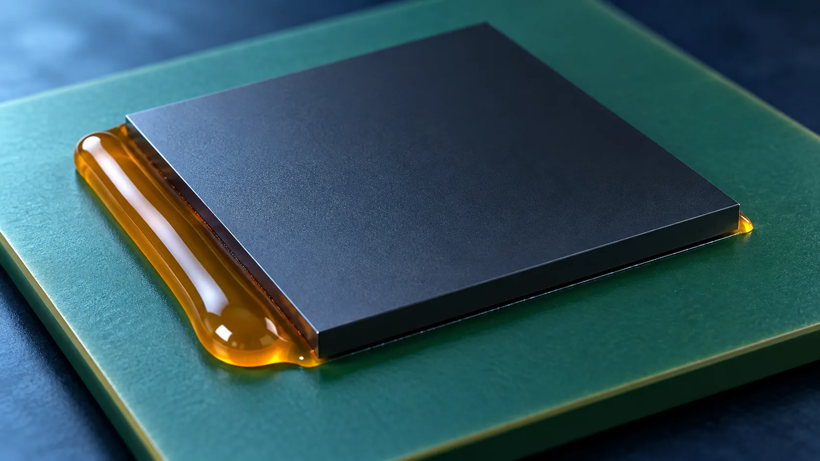
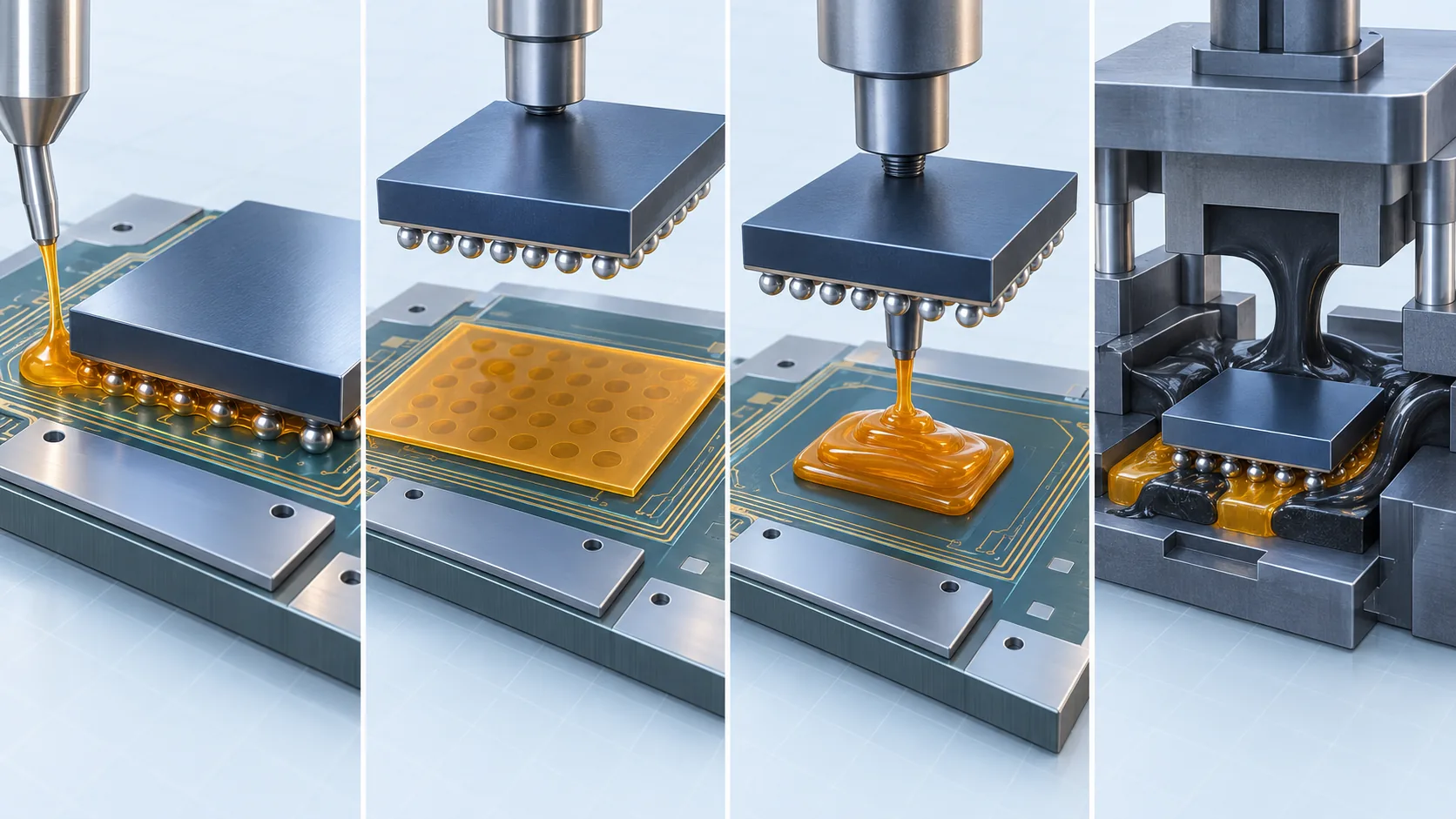
Sumitomo Bakelite gives its reason for developing a granular material: liquid resin "fills narrow gaps well, but has tended to give greater package warpage, and has issues of productivity and cost"Sourced. Easy flow, low warpage, low cost — you cannot have all three at once, which is why the methods have not converged (Commentary).
4. A materials engineer's view 1: filler particle size sets the gap you can fill
Both encapsulant and underfill are epoxy resin loaded heavily with silica powder (filler). The filler is there to bring CTE down, carry heat away and raise strength.
But filler has one very blunt side effect. A particle bigger than the gap does not go in.
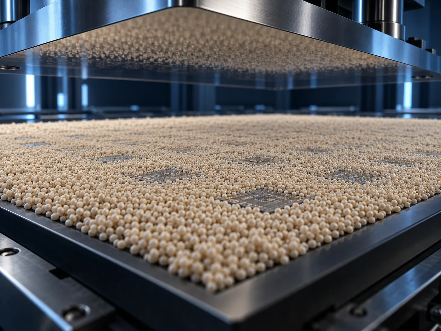
For its granular material aimed at 3DS-TSV (three-dimensional stacked DRAM connected by through-silicon vias), Sumitomo Bakelite states that "a compression-moulding encapsulant (granular) applying a 5 um cut filler" has made "filling the narrow regions of 3DS-TSV possible", and that a 3 µm cut granular material is now in developmentSourcedNot yet confirmed.
The important detail is that it says "5 µm cut", not "5 µm mean". What blocks a gap is not the average particle but the largest particle at the tail of the distribution. One oversized grain in ten thousand is enough: if the flow stops there, the fill has failed.
So managing filler is a contest about how large a particle you managed to remove, not about how large the particles are. Precision in classification, and dispersion that avoids agglomeration. The technology of making powder is what sets the package's limit (Commentary).
And here is the trade-off. Finer filler raises viscosity at the same loading, because surface area goes up. Harder to flow, and the very purpose — getting into a narrow gap — recedes. When Sumitomo Bakelite writes of its PLP granular material that it works "by optimising the filler size and the resin viscosity of the encapsulant", it means those two are being tuned togetherSourced (Commentary).
5. A materials engineer's view 2: above Tg the material is a different material
An encapsulant datasheet quotes two coefficients of thermal expansion. For Resonac's epoxy encapsulant for organic substrates (the CEL series) they are as followsSourced.
| Property | Value | What it means |
|---|---|---|
| CTE alpha-1 | 6 to 12 ppm/°C | Expansion below the glass transition temperature |
| CTE alpha-2 | 27 to 45 ppm/°C | Expansion above the glass transition temperature |
| Glass transition temperature Tg | 120 to 155 °C | The temperature where the resin goes from hard to soft |
| Flexural modulus | 16 to 27 GPa | How stiff it is |
| Moulding shrinkage | 0.08 to 0.35 % | How much it shrinks as it sets |
From the property table of Resonac's "Epoxy encapsulant for organic substrates" [Source 4]. The right-hand column is this article's explanation.
Alpha-2 is three to four times alpha-1. In other words, the same material expands in a different way either side of Tg.
Take the cumulative expansion of an encapsulant heated from 25 °C to a reflow peak of 260 °COur calculation.
- 25 °C to 140 °C (up to Tg): 115 °C × 9 ppm/°C = 1,035 ppm
- 140 °C to 260 °C (past Tg): 120 °C × 36 ppm/°C = 4,320 ppm
- Total = 5,355 ppm = 0.54 %
Had alpha-1 held across the whole range, it would be 235 °C × 9 ppm/°C = 2,115 ppm = 0.21 %. A factor of about 2.5.
On a 50 mm package edge, 0.54 % is about 270 µm. With alpha-1 alone it is about 106 µm. The difference is over 160 µmOur calculation. Seen from the 30 µm pitch joints covered in the Bumps article, that is not a negligible amount.
Assumptions: alpha-1, alpha-2 and Tg are representative values chosen from Resonac's published ranges, not values for a specific product. The 260 °C peak is our assumption. Real parts are constrained, so they do not expand as freely as this.
The calculation implies that pushing Tg above reflow temperature would halve the expansion. So why does the Tg of encapsulant for organic substrates sit at 120 to 155 °CSourced?
Because Tg and modulus move together. Raising Tg means raising crosslink density. More crosslinks, more stiffness. A stiff material cannot shed stress by deforming. Less expansion, and yet possibly more stress.
When Resonac writes of its granular EMC "CEL-400ZHF40" that it "combines low thermal expansion of 10 ppm/°C or less with a low modulus of 20 GPa or less", the selling point is exactly that pairing: expand little, but do not get too stiffSourced. Either one alone is not hard. Having both is — as is usually the way with materials (Commentary).
6. A materials engineer's view 3: the same material, developed both stiffer and softer
So far we have left the question of stiff versus soft open. As it happens, the materials makers have not narrowed it to one answer either.
Resonac develops CUF in two variants, according to where it goesSourced.
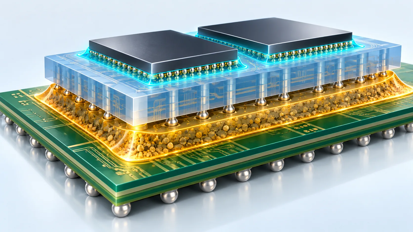
On CUF for Bottom, Resonac writes the followingSourced.
"For the next generation we are aiming at still lower CTE while working on development in both directions at once: higher modulus for stronger protection, and lower modulus to give the flexibility that follows warpage, so as to build a capability to supply CUF that answers a diverse set of needs."
Higher modulus and lower modulus, in the same sentence. That is not a slip. Which one is right depends on how the package fails.
- If the bumps fail first, you want the resin to hold them firmly (high modulus)
- If warpage is large, you want the resin to go along with it (low modulus)
Which is to say the material has no single optimum. So a materials supplier answers not with one best product but with a range — which is what the phrase "a capability to supply CUF that answers a diverse set of needs" is telling youSourced.
This is exactly the shape of the wire materials in the Bonding article, where gold, silver, copper and aluminium coexist, and of the socket materials in the Test article. Back-end materials do not converge on one winner. They branch by application (Commentary).
7. What is still hard
(1) The heat resistance required varies enormously by application
Same "epoxy plus silica", and yet the Tg needed differs completely depending on where it is going.
On 1 June 2026, Sumitomo Bakelite announced volume production of the "G785 series", an encapsulant for SiC power modules achieving "Tg 230 °C" in a solid epoxy resinSourced. The earlier G720 and G780 series are both at 195 °CSourced. The background is that "SiC semiconductors can operate at high temperature (above 200 °C)"Sourced.
SiC can run above 200 °C. But if the encapsulant's Tg is 195 °C, the resin softens beyond that point. The device's capability cannot be used.
In this situation, then, it is the encapsulant's limit, not the semiconductor's, that sets the ceiling for the system. Raising Tg from 195 °C to 230 °C looks like modest work, and yet it bears directly on making power modules smaller, which is to say denser in output — which is how the company positions itSourced (Commentary).
(2) Make it bigger and it warps
As the PLP article covered, the shortest route to higher productivity is a bigger panel. Sumitomo Bakelite gives the reason: "chips in advanced semiconductors are getting larger, and to raise productivity there is growing demand to move from wafer-level packaging (WLP), which loses many chips per wafer, to PLP, which yields more"Sourced.
But the larger the area, the larger the warpage that the CTE mismatch produces. The company's granular material "reduces panel warpage after moulding by optimising the filler size and the resin viscosity of the encapsulant", giving "uniform moulding even on large panels of 600 × 600 mm", which is its answer to that problemSourced.
(3) Liquid and solid each have their weaknesses
Of liquid resin the company says "it fills narrow gaps well, but has tended to give greater package warpage, and has issues of productivity and cost"Sourced.
A material that flows easily tends to lose out on shrinkage and warpage as it sets. Which is why liquid, film and granular forms all persist. When Resonac writes of its film-form EMC (the EB series) that it "eliminates local distortion arising from thickness variation", that too is a case of form being performanceSourced.
(4) Radioactive impurity, one more thing to control
The Bumps article covered alpha particles and soft errors. The same requirement reaches the encapsulant. Shinko Electric states that for MUF packages it "offers low-alpha mould resin in its line-up"Sourced.
Encapsulant is the material that covers the chip directly. So even trace radioactive impurity in the silica filler becomes something to control (Commentary).
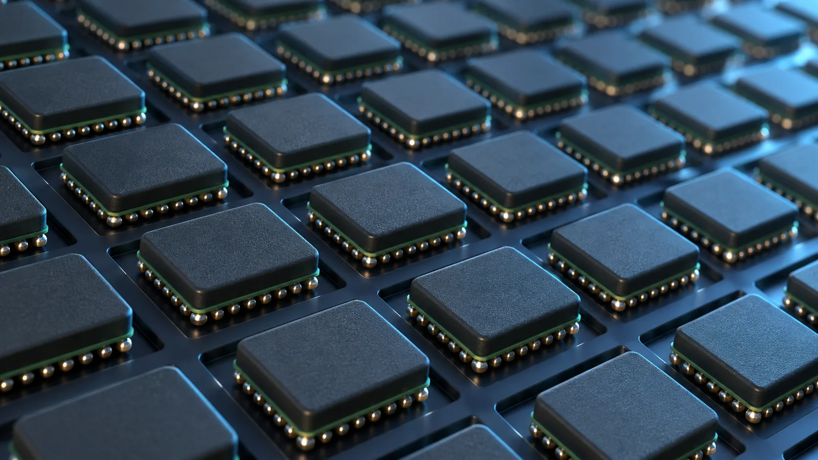
Underfill and encapsulant are the part of back-end assembly closest to the material itself. And the properties in play come down to a surprisingly small set.
- Particle size: how narrow a gap you can get into (5 µm cut, 3 µm cut in development)
- CTE: how far you close the gap with the neighbours (and there are two of them, alpha-1 and alpha-2)
- Tg: up to what temperature it stays hard (120 to 155 °C / 195 °C / 230 °C)
- Modulus: hold it down, or follow it (16 to 27 GPa / 20 GPa or less)
These four interfere with one another. Finer particles raise viscosity; higher Tg means stiffer; more filler to lower CTE makes it flow less still. Developing underfill and encapsulant is the work of answering that four-way tug of war, application by application (Commentary).
8. Glossary
- Underfill
- The resin that fills the gap between chip and substrate and relieves stress on the bumps.
- Encapsulant (EMC)
- Epoxy Molding Compound. The resin that covers the chip and its surroundings together.
- CUF
- Capillary Underfill. Liquid placed after bonding and drawn into the gap by capillary action.
- MUF
- Mold Under Fill. Moulding and gap filling done together in a single step.
- NCF
- Non-Conductive Film. Film-form resin placed in advance of bonding.
- Granular material
- Encapsulant supplied as powder or granules. Compression moulding gives uniform coverage over a large area.
- Compression moulding
- Spreading resin and pressing it with a mould.
- Transfer moulding
- Forcing melted resin into a mould cavity.
- Filler
- Inorganic powder mixed into the resin, mostly silica. It lowers CTE, carries heat and raises strength.
- Cut size
- A statement that the maximum filler particle size has been cut at a given value, as in "5 µm cut".
- CTE
- Coefficient of Thermal Expansion, in ppm/°C.
- alpha-1 and alpha-2
- CTE below Tg is alpha-1, above Tg is alpha-2. Alpha-2 is the larger.
- Tg
- Glass transition temperature. Where the resin goes from hard to soft.
- Modulus
- Resistance to deformation under load. Higher means stiffer.
- Moulding shrinkage
- How much the material shrinks as it sets. One cause of warpage.
- Void
- A cavity left inside the filled resin.
- Unfilled area
- Where the resin has not reached the far corners and the gap stays open.
- Warpage
- Deformation of the package caused by CTE mismatch or moulding shrinkage.
- Low-alpha material
- A material with reduced radioactive impurity emitting alpha particles, used against soft errors.
- 3DS-TSV
- Three-dimensional stacked DRAM connected by through-silicon vias. Filling its narrow regions is the challenge.
- UL-94 V-0
- One rating class in the flammability standard for plastics.
9. Primary sources
- Resonac "Manufacturing processes for advanced semiconductor packages and the materials used in them" (Japanese-language page) — resonac.com
- Resonac "Materials that help suppress warpage and relax stress in advanced semiconductor packages, part 2" (Japanese-language page) — resonac.com
- Resonac "Materials that help suppress warpage and relax stress in advanced semiconductor packages, part 3" (Japanese-language page) — resonac.com
- Resonac "Epoxy encapsulant for organic substrates" (Japanese-language page) — resonac.com
- Resonac "Liquid encapsulant for flip chip" (Japanese-language page) — resonac.com
- Shinko Electric "Mold underfill packages" (Japanese-language page) — shinko.co.jp
- Sumitomo Bakelite "Epoxy moulding compounds for semiconductor encapsulation, SUMIKON® EME" (Japanese-language page) — sumibe.co.jp
- Sumitomo Bakelite "Compression-moulding encapsulant (granular) for 3DS-TSV now on sale", 31 May 2024 (Japanese-language release) — sumibe.co.jp
- Sumitomo Bakelite "Volume production of a compression-moulding encapsulant (granular) for advanced-semiconductor PLP", 19 November 2024 (Japanese-language release) — sumibe.co.jp
- Sumitomo Bakelite "An industry first: volume production begins on the G785 series encapsulant for SiC power modules, achieving a world-class Tg of 230 °C in a solid epoxy resin", 1 June 2026 (Japanese-language release) — sumibe.co.jp
10. Claim-to-source audit
| Claim in the text | Basis | Label |
|---|---|---|
| That underfill is "a polymer material that seals and reinforces the gap between chip and substrate, relieving the stress on the solder bumps that comes from thermal cycling and the like" | Resonac technical column 003[Source 1] https://www.resonac.com/jp/solution/column/003.html | Sourced |
| That granular EMC "CEL-400ZHF40" combines low thermal expansion of 10 ppm/°C or less with a low modulus of 20 GPa or less; that film EMC (EB series) eliminates local distortion arising from thickness variation and cures at low temperature | Resonac technical column 008[Source 2] https://www.resonac.com/jp/solution/column/008.html | Sourced |
| That CUF is filled into the gaps between members with large CTE differences and distributes stress across the whole area; the requirements given for CUF for Top (high flow before cure, small filler that will not clog); the requirements given for CUF for Bottom (still lower CTE, plus development in both higher-modulus and lower-modulus directions, building a capability to answer diverse needs) | Resonac technical column 009[Source 3] https://www.resonac.com/jp/solution/column/009.html | Sourced |
| Properties of the epoxy encapsulant for organic substrates (CEL series): alpha-1 6 to 12 ppm/°C, alpha-2 27 to 45 ppm/°C, Tg 120 to 155 °C, flexural modulus 16 to 27 GPa, moulding shrinkage 0.08 to 0.35%; and that modulus and expansion are controlled to suppress package warpage | Resonac "Epoxy encapsulant for organic substrates"[Source 4] https://www.resonac.com/jp/products/semi-backend-process/76/012.html | Sourced |
| That MUF fills even where the chip-to-substrate gap is 45 µm or less; that fine filler is used and low-alpha mould resin is offered; that no resin dispense area is needed so package area can be reduced; that both solder bumps and Cu pillars are supported | Shinko Electric "Mold underfill packages"[Source 6] https://www.shinko.co.jp/product/package/assembly/muf.php | Sourced |
| That the roles of encapsulant are protecting the chip, insulation from the external environment, spreading heat from the chip and handleability during mounting; that both transfer and compression moulding are supported; that UL-94 V-0 is achieved without flame retardant | Sumitomo Bakelite "SUMIKON® EME"[Source 7] https://www.sumibe.co.jp/product/it-materials/epoxy/sumikon-eme/ | Sourced |
| Announced 31 May 2024. That 3DS-TSV means three-dimensional stacked DRAM connected by through-silicon vias; that a compression-moulding encapsulant (granular) applying a 5 um cut filler made filling the narrow regions of 3DS-TSV possible; that a low-modulus resin was adopted and CTE controlled to reduce warpage; that liquid resin fills narrow gaps well but tends to give greater package warpage and has issues of productivity and cost | Sumitomo Bakelite news release, 31 May 2024[Source 8] https://www.sumibe.co.jp/topics/2024/it-materials/0522_02/index.html | Sourced |
| That a 3 µm cut granular material is in development (no production record confirmed) | Sumitomo Bakelite news release, 31 May 2024[Source 8] https://www.sumibe.co.jp/topics/2024/it-materials/0522_02/index.html | Not yet confirmed |
| Announced 19 November 2024. That the granular material reduces panel warpage after moulding by optimising filler size and resin viscosity; that uniform moulding is possible even on large panels of 600 × 600 mm; that chips in advanced semiconductors are getting larger and demand is shifting from WLP to PLP for better yield per panel | Sumitomo Bakelite news release, 19 November 2024[Source 9] https://www.sumibe.co.jp/topics/2024/it-materials/1118_01/ | Sourced |
| Announced 1 June 2026. That the G785 series achieves Tg 230 °C; that the earlier G720 and G780 series are both at 195 °C; that SiC semiconductors can operate at high temperature above 200 °C; that this is positioned as contributing to smaller, higher-power-density modules | Sumitomo Bakelite news release, 1 June 2026[Source 10] https://www.sumibe.co.jp/topics/2026/it-materials/0428_01/index.html | Sourced |
| That the liquid encapsulant for flip chip, CEL-C-3900 series, is a non-filler type with good impregnation and migration resistance, cured at 120 °C / 15 min + 150 °C / 1 h; and that the CEL-C-3730 series has good adhesion under humidity, cured at 150 °C / 2 h or 165 °C / 2 h | Resonac "Liquid encapsulant for flip chip"[Source 5] https://www.resonac.com/jp/products/semi-backend-process/76/015.html | Sourced |
| Fig. 6: cumulative expansion from 25 °C assuming alpha-1 = 9 ppm/°C, alpha-2 = 36 ppm/°C, Tg = 140 °C and a 260 °C peak (1,035 ppm to Tg, 4,320 ppm beyond, 5,355 ppm = 0.54% in total); 2,115 ppm = 0.21% if alpha-1 held throughout, a factor of about 2.5; about 270 µm against about 106 µm on a 50 mm edge | Our calculation. Alpha-1, alpha-2 and Tg are representative values chosen from Resonac's published ranges, not values for a specific product. The 260 °C peak is our assumption. It is free expansion, not the behaviour of a constrained real part[Source 4] https://www.resonac.com/jp/products/semi-backend-process/76/012.html | Our calculation |
| That the three rows in Fig. 9 differ in metric: the top two are encapsulant glass transition temperatures and the bottom is a semiconductor's operating temperature | Our note in this article. The numbers themselves come from Sources 4 and 10[Source 4] https://www.resonac.com/jp/products/semi-backend-process/76/012.html[Source 10] https://www.sumibe.co.jp/topics/2026/it-materials/0428_01/index.html | Commentary |
| The observation that underfill and encapsulant belong to a close material family; the reading that the resin is a structural part sharing stress rather than an adhesive; the explanation that a "5 µm cut" is a maximum rather than a mean and that classification and dispersion precision set the package's limit; that finer filler raises surface area and so viscosity; that raising Tg raises crosslink density and stiffness so stress cannot be shed; the reading that demanding both higher and lower modulus shows there is no single optimum; the observation that in SiC the encapsulant's limit sets the system ceiling; the framing of particle size, CTE, Tg and modulus as four interfering properties | Commentary: this article's organisation and reading of published content. It is not a view expressed by any of the companies | Commentary |
| That the cross-sections in Figs. 1, 2, 4, 5 and 8 are drawings for explanation rather than observed images | Our note in this article | Commentary |
Last updated 20 September 2026. Sources are limited to primary material (official product pages, technical columns and news releases from materials and package manufacturers). Because the article contains readings about materials design, those passages are marked Commentary to separate them from sourced fact. All figures are explanatory concept graphics. Visual-overview figures are shown as AI-generated conceptual images, matching the Japanese edition. Vector drawings are retained where they carry quantitative values or precision-critical technical labels. AI-generated images do not depict real equipment, products, facilities, dimensions or exact cross-sections; replaced source SVG overview drawings remain in the HTML but are hidden.