TECHNOLOGY EXPLAINER
What Die Stacking Is
— why the industry stopped laying chips out side by side
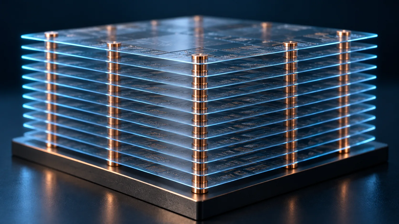
Stack the chips vertically. Simple to say, but behind it sits one very specific goal — shortening the wiring by a factor of a hundred — and one very extreme piece of machining: grinding silicon down to five micrometres.
- What stacking is (the short version)
- Why stack vertically — the three reasons imec gives
- What actually changes when you stack instead of spread
- Stacking spans eight orders of magnitude
- What stacking requires first: thinning
- A materials engineer's view: what thinning costs you
- The problem stacking creates: heat
- What is still hard
- Glossary / Primary sources / Claim-to-source audit
Sourced = a value stated in published material from a research institute or manufacturer (link given)
Our calculation = a figure this article derived, with the assumptions spelled out
Not yet confirmed = research-stage work or a plan with no confirmed production record
1. What stacking is (the short version)
Stacking means connecting several chips by placing them one above another rather than side by side on a plane.
- What gets stacked: identical dies (DRAM on DRAM, which is HBM) or different ones (logic under memory)
- How they connect: electrodes that pass through the chip (TSVs), or direct face-to-face bonding
- What for: shorter wiring, less area, more bandwidth
The HBM article is about stacking memory; the Hybrid Bonding article is about the joining method that makes fine-pitch stacking possible. This article is about the act of stacking itself: why you would, how fine it can go, and what you give up to do it.
2. Why stack vertically — the three reasons imec gives
imec sets out three motivations for 3D IC stackingSourced (imec).
| Reason | How imec puts it |
|---|---|
| 1. Break the memory wall | Provide a shorter path between processor and memory |
| 2. Add functionality | Increase functionality in an IC that is constrained in size |
| 3. Improve yield | Improve the yield of large, complex systems |
imec also notes that different process technologies can be used for different subsystems, optimising design cost and yieldSourced.
3. What actually changes when you stack instead of spread
The most fundamental difference is the distance between chips.
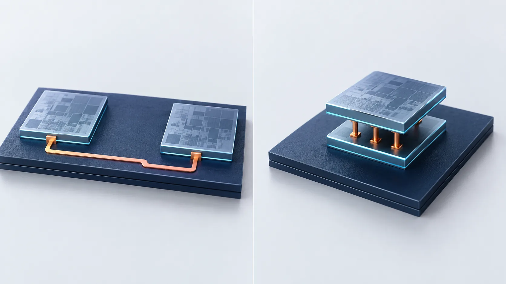
The longer the wire, the more resistance and capacitance it carries, and the slower and blunter the signal becomes. The only way to compensate is a stronger driver circuit at the sending end, which costs power.
For its 3D V-Cache technology, AMD reports that direct copper-to-copper, bumpless construction delivers more than 200 times the interconnect density of on-package 2D chiplets, more than 15 times the interconnect density of 3D approaches using solder bumps, and more than three times the energy efficiency per connectionSourced (AMD). Shortening the connection comes straight back as energy efficiency.
4. Stacking spans eight orders of magnitude
"Stacking" is one word, but how fine the connection pitch is makes it an entirely different technology. imec frames that range as covering roughly eight orders of magnitudeSourced (imec).
Volume production today saturates at roughly 30 µm pitch, as imec puts itSourced.
So the right half of the chart (30 µm and coarser) is the world already in production, and the left half (a few µm and finer) is the world still to be crossed into. Sitting on the boundary is hybrid bonding, which abandons solder and joins copper directly (covered in the Hybrid Bonding article).
Progress in stacking technology is movement leftward across this chart.
5. What stacking requires first: thinning
Stacking has one unavoidable prerequisite: the chips have to be thin.
There are two reasons. First, the total height of the stack has to fit in the package. Second, an electrode that passes right through the die (a TSV) is easier to make the less material it has to pass through.
How thin is possible
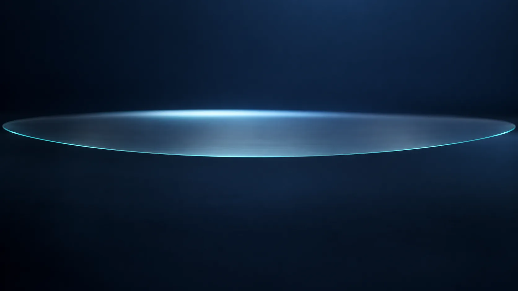
DISCO gives an example of thin-finish grinding taking a 300 mm silicon wafer down to 5 µmSourced (DISCO).
The ratio of diameter to thickness is 60,000 to 1Our calculation. Scale a sheet of 0.09 mm copier paper to the same ratio and you get a disc 5.4 m acrossOur calculation. Now carry it without breaking it, and bond it to something. That is the world thinning operates in.
The TAIKO process — leaving the rim behind
How do you handle a wafer that thin? DISCO's TAIKO process answers the question structurally.
In the company's words, TAIKO is a technique that grinds and thins only the inner region of the wafer, leaving the outermost edge (about 3 mm) intactSourced (DISCO).
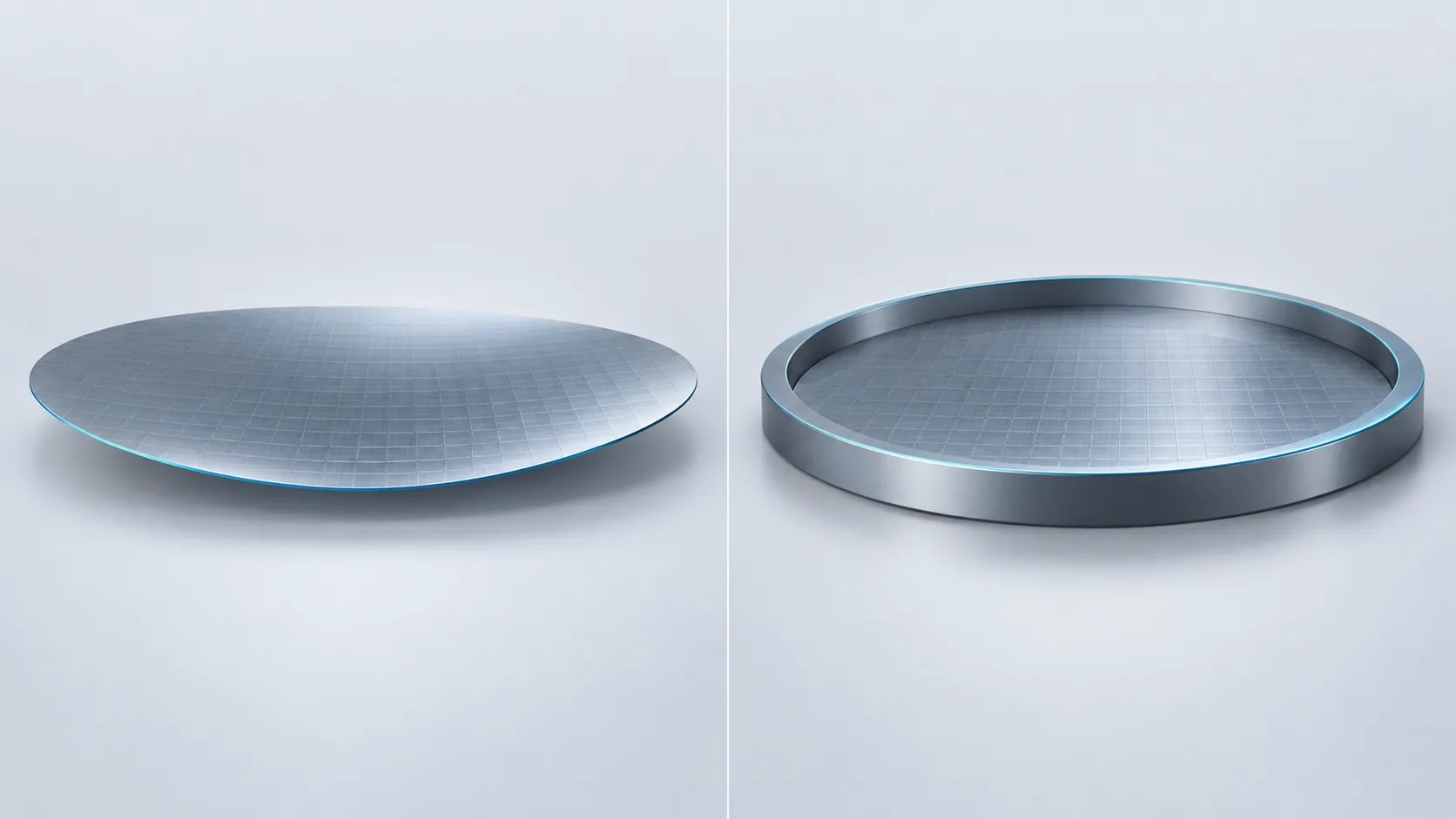
You want the wafer thin, and yet you deliberately leave 3 mm of rim untouched. At first glance that looks like a half-finished job. But that rim works like an embroidery hoop, holding the thin centre in shape.
Not a stronger material, not a more precise machine — the problem is solved with geometry. It is a good example of process craft.
6. A materials engineer's view: what thinning costs you
Thinning is not simply removal. Taking material away changes the properties of what is left.
(1) It gets weaker
DISCO frames the challenge as safely handling a wafer whose mechanical strength has been reduced by thinning to the point where it breaks very easilySourced.
(2) The edge turns into a blade
The company explains that as the wafer is thinned, the rounded edge profile becomes a sharp shape and its mechanical strength drops sharply, so that chipping occurs and becomes a cause of wafer breakageSourced. The countermeasure given is an edge trimming process.
The outer edge of a silicon wafer is machined to a rounded cross-section specifically to prevent chipping. Grind the wafer from above, though, and only the lower half of that curve survives, leaving something like a knife edge. The shape that existed to prevent breakage becomes the cause of it once the wafer is thinned — and that structural irony is exactly why an edge trimming step exists.
(3) The ground surface carries damage
Grinding leaves a damaged subsurface layer. DISCO describes stress relief technology that removes this damaged layer to improve die bending strength further, naming dry etching and dry polishingSourced.
Mechanical grinding is fast but leaves damage. Damage is where cracks start. So after grinding, the surface is reconditioned chemically and mechanically.
This is the same shape of argument as the CMP discussion in the Hybrid Bonding article. Whether you are bonding a surface or thinning one, it ends in the same question: how good a surface can you produce? Stacking technology is, in practice, a stack of surface-making technologies.

7. The problem stacking creates: heat
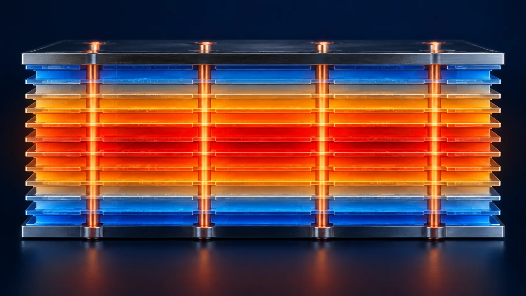
Stacking has one unavoidable side effect: heat has fewer ways out.
Laid out on a plane, every chip touches a cooler from above. Stacked, the lower layers have the upper ones as a lid.
There is a twist here. Being thin helps thermally and hurts thermally at the same time.
It helps: a thinner layer lets heat through more readily in the vertical direction, because the distance is shorter.
It hurts: a thinner layer has less cross-section to spread heat laterally.
A local hot spot cannot be diluted by spreading it across the plane.
In other words, thinning is good for conducting heat through and bad for spreading it out (our commentary). The difficulty of thermal design in stacked assemblies comes from that double-sidedness.
Answering it structurally: AMD's second-generation 3D V-Cache
For the second generation of 3D V-Cache, AMD moved the cache die below the compute cores, inverting the design so that the cores sit directly against the coolerSourced. The company states that a chip that runs cooler can run faster, and reports that the Ryzen 7 9850X3D gained 400 MHz of boost clock over the previous generationSourced (AMD).
No change to the circuits, the bonding method or the process — 400 MHz from swapping top and bottom. In stacking, "in what order" matters as much as "what". And the criterion that settled it was not performance. It was heat.
8. What is still hard
(1) Yield multiplies
As the HBM article notes, in a stack one bad die makes the whole stack bad. The more layers, the lower the probability that every one of them is good.
(2) You cannot tell good from bad before stacking
The remedy is to test each die before it goes into the stack, but testing an ultra-thin die without damaging it is itself difficult.
(3) Stress
Thin dies are stacked, encapsulated, and cycled through heating and cooling. The more layers of materials with different thermal expansion, the more complicated the stress picture becomes.
(4) The pitch wall
As Section 4 showed, imec describes volume production as saturating at roughly 30 µm pitchSourced. A few micrometres and below has been demonstrated in research, but meeting cleanliness, alignment and equipment requirements simultaneously at production level remains the open problem (covered in the Hybrid Bonding article).
9. Glossary
- Stacking
- Connecting chips by placing them one above another. The core of 3D assembly.
- 2.5D
- Chips laid out on a plane and connected through a shared platform.
- 3D
- Chips stacked vertically and connected.
- TSV
- Through-Silicon Via. The electrode that links stacked chips vertically.
- Thinning (backgrinding)
- Grinding the back of the wafer to reduce its thickness.
- TAIKO process
- Thinning only the inner region while leaving a rim of about 3 mm.
- Edge trimming
- Removing the rounded wafer edge before thinning, to prevent it becoming sharp.
- Damaged subsurface layer
- The layer of machining damage left near the surface by grinding.
- Stress relief
- Removing the damaged layer to restore strength, for example by dry etching.
- Bending strength
- Resistance to bending. Especially important for thin dies.
- D2W
- Die-to-Wafer. Bonding singulated dies onto a wafer.
- W2W
- Wafer-to-Wafer. Bonding whole wafers together.
- Pitch
- The spacing between connection points. Finer pitch means more connections.
- Memory wall
- The problem of memory not supplying data fast enough for the available compute.
- 3D V-Cache
- AMD's technology for stacking a cache die onto a compute die.
10. Primary sources
- imec "3D integration: IC stacking to extend scaling" — imec-int.com
- imec "A view on the 3D technology landscape" — imec-int.com
- imec "imec demonstrates die-to-wafer hybrid bonding with Cu interconnect pad pitch of 2um", 29 May 2024 — imec-int.com
- DISCO "Thin finish grinding" (Japanese-language page) — disco.co.jp
- DISCO "TAIKO process" (Japanese-language page) — disco.co.jp
- AMD "AMD 3D V-Cache Technology" — amd.com
11. Claim-to-source audit
| Claim in the text | Basis | Label |
|---|---|---|
| The three motivations for 3D stacking (a shorter path between processor and memory, more functionality within a size constraint, better yield for large systems), and the point that different process technologies can be used for different subsystems | imec 3D integration page[Source 1] https://www.imec-int.com/en/expertise/cmos-advanced/connect/3d-integration | Sourced |
| The pitch hierarchy: package stacking at mm class; 2.5D and chiplets saturating in production at about 30 µm; Sn microbumps demonstrated at 7 µm with 5 µm next; D2W hybrid bonding down to 3 µm; W2W targeting 700 nm and 500 nm; transistor stacking below 100 nm. Roughly eight orders of magnitude overall | imec "A view on the 3D technology landscape"[Source 2] https://www.imec-int.com/en/articles/view-3d-technology-landscape | Sourced |
| D2W hybrid bonding demonstrated at 2 µm pitch | imec press release, 29 May 2024[Source 3] https://www.imec-int.com/en/press/imec-demonstrates-die-wafer-hybrid-bonding-cu-interconnect-pad-pitch-2mm | Sourced |
| An example of grinding a 300 mm silicon wafer down to 5 µm | DISCO "Thin finish grinding"[Source 4] https://www.disco.co.jp/jp/solution/library/grinder/thin.html | Sourced |
| That thinning reduces mechanical strength and makes wafers break easily; that thinning turns the rounded edge into a sharp profile whose weakness causes chipping and breakage; that edge trimming is the countermeasure; that removing the damaged subsurface layer by dry etching and dry polishing is stress relief technology that improves die bending strength | DISCO "Thin finish grinding"[Source 4] https://www.disco.co.jp/jp/solution/library/grinder/thin.html | Sourced |
| TAIKO grinds only the inner region, leaving about 3 mm of rim. The listed benefits are less warpage, higher strength, easier handling, zero edge chipping, no outgassing after high-temperature steps, and fewer particles carried in | DISCO "TAIKO process"[Source 5] https://www.disco.co.jp/jp/solution/library/grinder/taiko_process.html | Sourced |
| AMD 3D V-Cache: more than 200 times the interconnect density of 2D chiplets and more than 15 times that of solder-bump 3D, with more than three times the energy efficiency per connection. The second generation moves the cache below the cores so the cores face the cooler. The Ryzen 7 9850X3D gains 400 MHz of boost clock | AMD product technology page[Source 6] https://www.amd.com/en/products/processors/technologies/3d-v-cache.html | Sourced |
| The ratio of 300 mm diameter to 5 µm thickness is 60,000 to 1; scaling 0.09 mm paper by the same ratio gives a disc 5.4 m across | Our calculation: 300 divided by 0.005, and 0.09 multiplied by 60,000 | Our calculation |
| A few millimetres when laid out side by side versus tens of micrometres when stacked, about a hundredfold | Our approximation based on representative orders of magnitude. Not values for any specific product | Our calculation |
| That thinning helps vertical heat conduction but hurts lateral heat spreading; that the rounded wafer edge sharpens when thinned; that stacking multiplies yield | Commentary based on general relationships in physics and materials engineering. No specific numerical claim is made | Commentary |
Last updated 20 September 2026. Sources are limited to primary material (official publications and product technology pages from research institutes and manufacturers). All figures are explanatory concept graphics. Visual-overview figures are shown as AI-generated conceptual images, matching the Japanese edition. Vector drawings are retained where they carry quantitative values or precision-critical technical labels. AI-generated images do not depict real equipment, products, facilities, dimensions or exact cross-sections; replaced source SVG overview drawings remain in the HTML but are hidden.