TECHNOLOGY EXPLAINER
What Semiconductor Test Is
— the step that decides what can be sold, and the materials behind it
A semiconductor is not yet a product the moment it is finished. Current has to be pushed through every one of them and each confirmed good before anything can ship. That confirming step has become one of the most congested places in the whole AI-chip supply chain. And what actually decides the outcome on the floor is materials: needles, springs and resins.
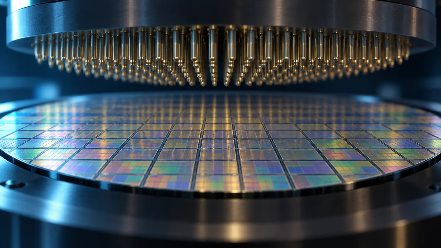
- What test is (the short version)
- Why test is needed — once it is cut, there is no going back
- Test does not happen once — a map of the flow
- The wafer test floor — probers and probe cards
- A materials engineer's view 1: the needle is a bundle of contradictory demands
- A materials engineer's view 2: the socket changes material part by part
- Test in the stacking era — KGD as a precondition
- What is still hard
- Glossary / Primary sources / Claim-to-source audit
Sourced = content stated in a company's published material or a published patent (link given)
Our calculation = a figure this article derived, with the assumptions spelled out
Not yet confirmed = a plan with no confirmed track record
Beyond those, process framing and readings about materials design are marked Commentary.
1. What test is (the short version)
Semiconductor test is the step that puts an electrical signal into a finished device, compares the waveform that comes back against the right answer, and decides whether the part is good or bad.
In its own description of the business, Advantest says a test system "compares the output waveform of a semiconductor against a reference and judges it good or defective"Sourced. It also says test systems are "used at the end of the wafer fabrication process, and again at final inspection after packaging and the rest"Sourced.
- What is being looked at: "whether the semiconductor operates properly, and whether it meets the performance and endurance being asked of it"Sourced
- When it happens: once while still a wafer, and again once it is packaged. Depending on the application, a test under applied heat and a test in something close to the real system are added on top
- What it is for: besides keeping bad parts from getting out, "to analyse the cause of failures and raise yield"Sourced
Test is usually pictured as one inspection bolted onto the end. It is not. It is inserted again and again along the flow, and each time it throws bad parts away. And the later the step, the more money has already gone into that chip. So you want to drop the bad ones as early as you possibly can — and that single motive explains most of the technology in the rest of this article.
2. Why test is needed — once it is cut, there is no going back
In the front end, hundreds or thousands of chips are built at the same time on a single silicon wafer. Across several hundred process steps, variation and defects inevitably creep in. They are never all good.
Japan Electronic Materials describes wafer test as the step that "decides whether the IC chips that have been made are good or defective, before the hundreds of IC chips laid out on the wafer are cut (diced) into chips a few millimetres square"Sourced.
The phrase that matters there is "before they are cut". Once a wafer has been diced, it can never be put back the way it was. If you know good from bad beforehand, the bad chips are simply discarded. Notice after dicing, and the substrate, the encapsulant, the joining material and the machine time spent assembling that chip are all wasted together.
Back-end materials — substrates, underfill, moulding compound, solder, adhesive film — ideally get used only on chips already judged good. If wafer test is loose and lets a bad die pass as good, the material spent on it is guaranteed waste. If test is too tight and calls a good die bad (overkill), you lose a chip that would have sold. How well test works feeds straight through to material yield.
3. Test does not happen once — a map of the flow
What gets called "test" in fact has a different name and a different machine at each stage. Here is the overall picture first.
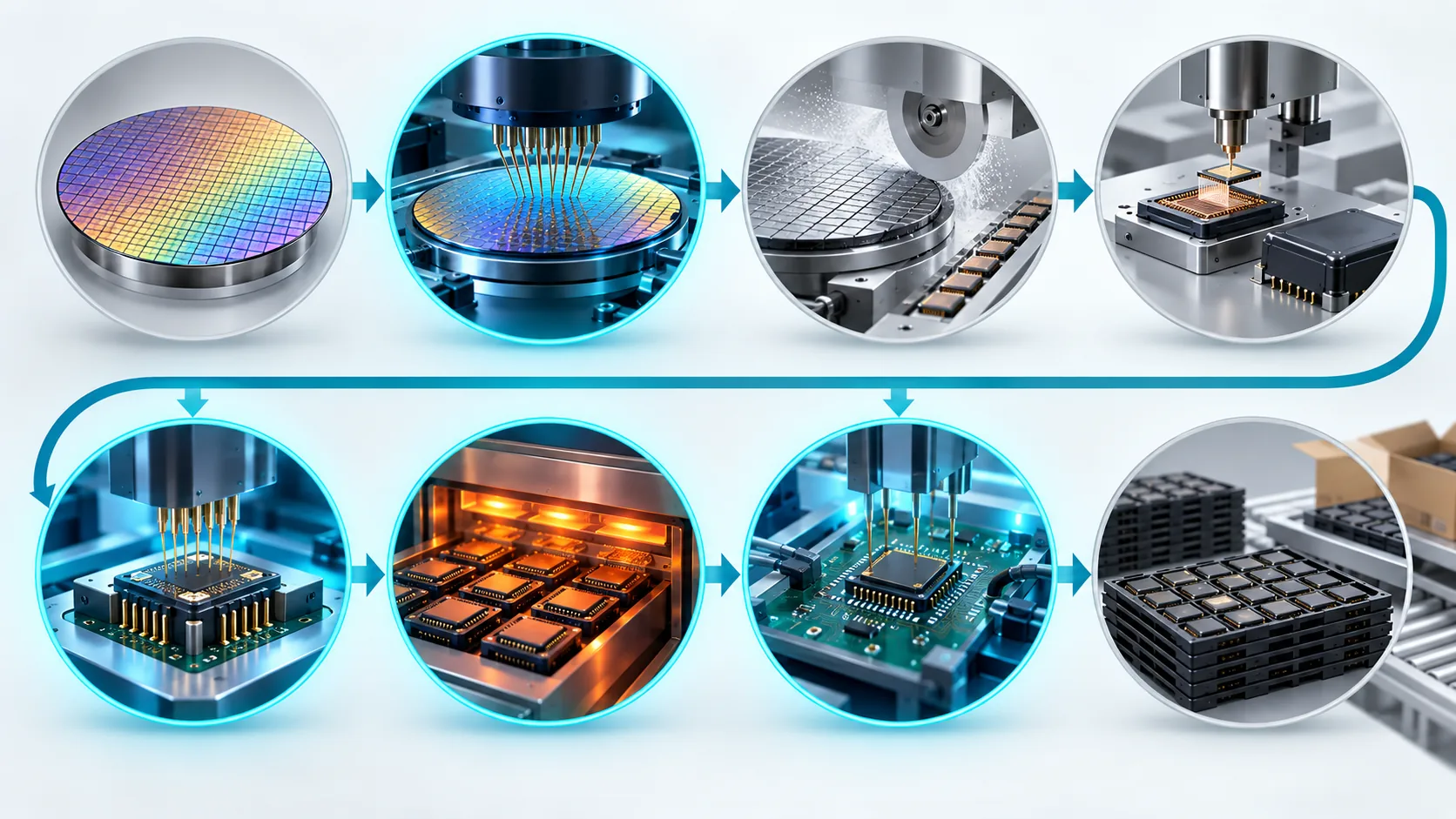
(1) Wafer test
Advantest describes wafer-level test as "testing carried out at the stage before the wafer is divided into individual dice", which "checks the electrical characteristics of each die on the wafer and helps find defects early"Sourced.
(2) Final test (package test)
By the same account this is "a test that confirms a packaged device operates correctly as a finished semiconductor device", and it "verifies that it operates stably under conditions such as temperature change"Sourced. A die that was good on the wafer can still fail after being cut, stacked, encapsulated and warped on its way through the back end.
(3) Burn-in
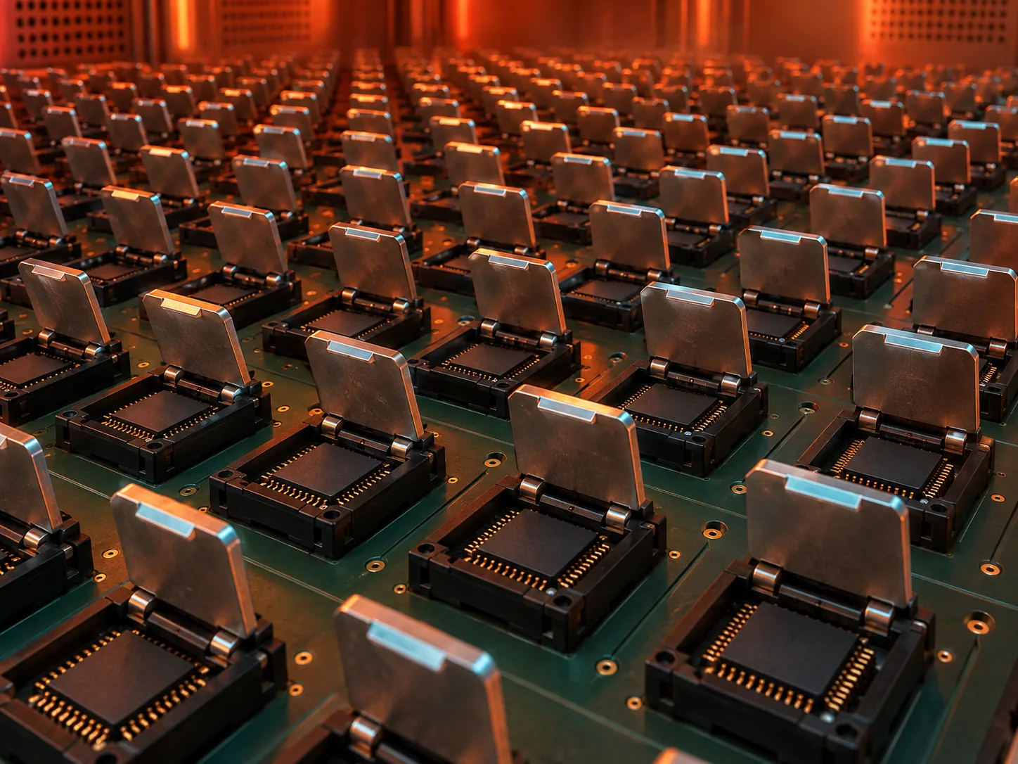
Yamaichi Electronics describes burn-in as "the temperature-and-voltage test carried out at the final stage of semiconductor manufacturing": several ICs are loaded onto a test board and "stressed with temperature and voltage for some hours in a high-temperature environment of 125 to 180 degrees Celsius, to screen out early-life failures"Sourced. The stated purpose is "two things: (1) higher reliability and (2) higher yield"Sourced.
The idea is simple. A chip with a disposition to fail fails sooner when you put heat and voltage through it. So before shipping you deliberately run it hard, and let the ones that are going to die early die here. Better broken in the factory than broken in the field.
(4) SLT (system level test)
Advantest describes SLT as "a test that runs an OS and software for verification on a platform reproducing operating conditions close to the real use environment of an end product such as a smartphone or a PC"Sourced. On its product pages the company positions SLT as "testing the behaviour of a semiconductor in the real use environment where it is built into a system or an end product", driven by "market demands such as testing increasingly complex devices, cutting test cost, and large-scale volume production"Sourced.
However finely a tester applies patterns, it cannot fully reproduce the state in which an OS is running, several chips are talking at once, and the supply rail is moving. SLT is the step that fills in the part which cannot be reproduced, using something close to the real machine.
4. The wafer test floor — probers and probe cards
Wafer test combines two pieces of equipment: the prober, which carries the wafer and aligns it, and the probe card, which actually touches the pads on the wafer.
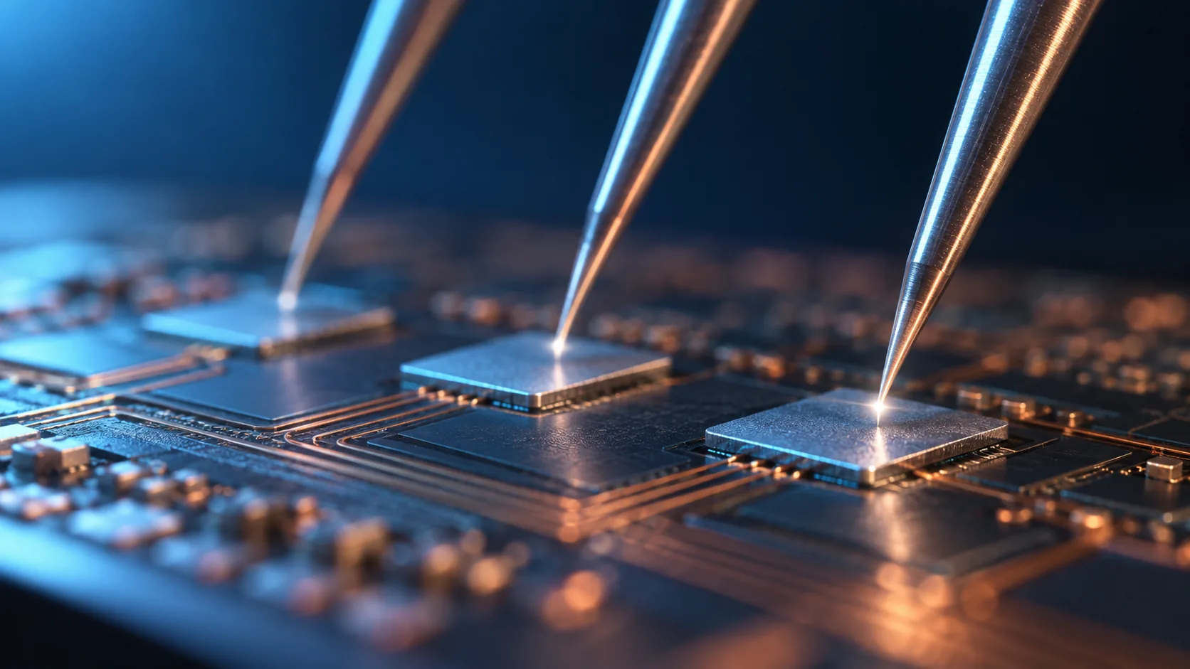
(1) The probe card — the connector between tester and chip
Micronics Japan defines a probe card as "a tool used for the electrical inspection of LSI chips formed on a silicon wafer, in the wafer inspection step of LSI (semiconductor integrated circuit) manufacture", and explains that it "is fitted to a wafer prober and acts rather like a connector joining the electrodes of the LSI chip to the LSI tester that does the measuring"Sourced. And then: "the needles of the probe card are brought into contact with the electrodes of the LSI chip, electrical inspection is carried out, and a good/bad judgement is made"Sourced.
Probe cards split into several types by how the needle is made. Japan Electronic Materials classifies its own products into M type (MEMS), V type (vertical) and C type (cantilever)Sourced.
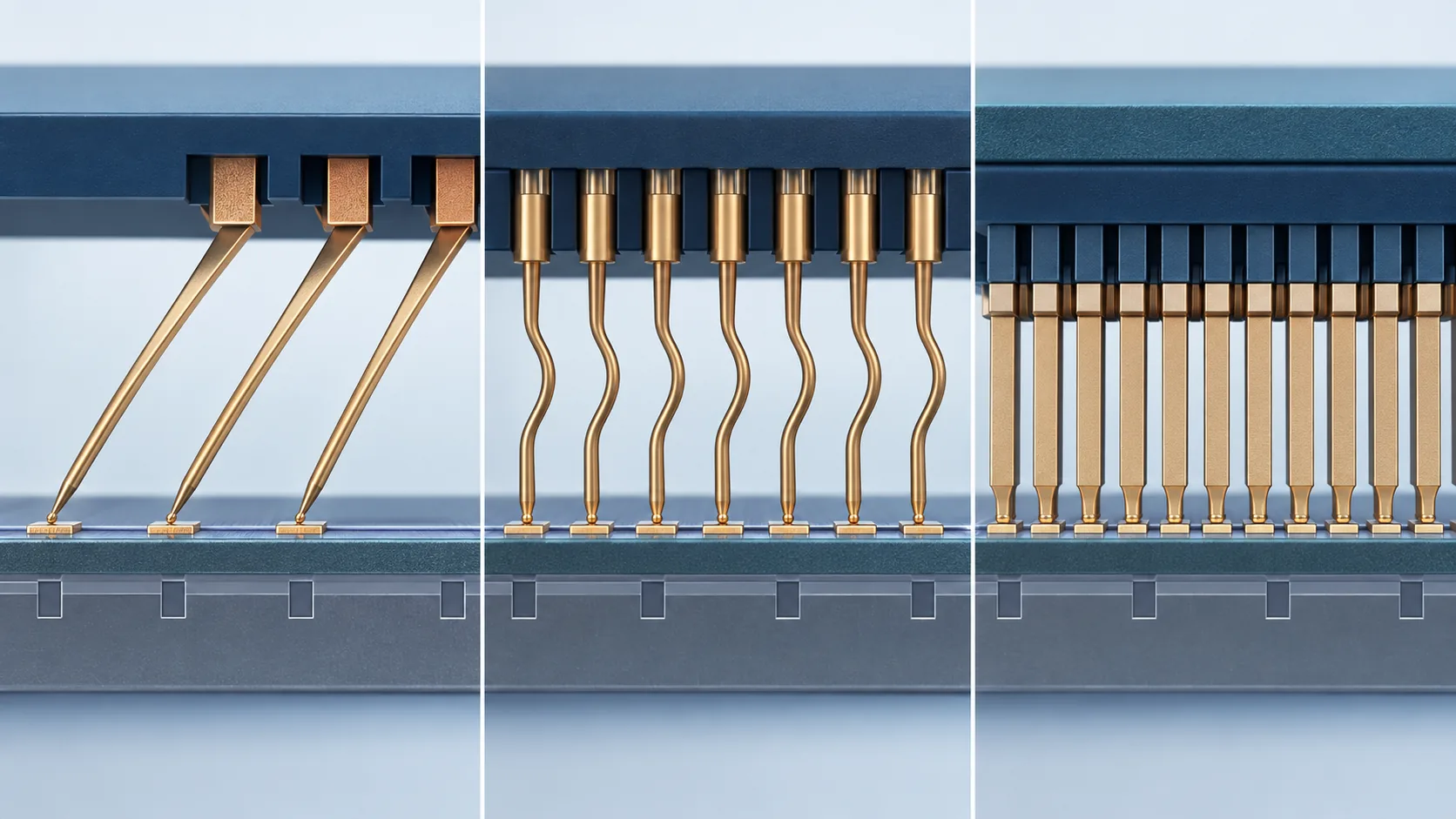
Micronics Japan's MEMS probe card, MEMS-V, is a "square needle type" using "a new MEMS probe in a high-hardness material, wear-resistant and long-lived", and is described as delivering "high probe positional accuracy and stable contact resistance", "excellent maintainability, with single-pin replacement made easy", and "capability for high- and low-temperature testing over a large probing area"Sourced.
(2) The prober — aligning to 0.8 micrometres while taking a tonne
Tokyo Electron's wafer prober Prexa MS is a fully automatic 300 mm wafer prober. Noting that for leading-edge DRAM "the test pin count and the heat generated are both increasing", the company states that it "handles an ultra-high load capacity of up to 1000 kg" and "enables full-wafer test (single-touchdown contact) for coming memory devices"Sourced. Positioning accuracy is published as XY ±0.8 µm and Z ±2.5 µm (±5.0 µm as an option)Sourced. It is also said to carry "heat-absorption control for high heat generation"Sourced.
That figure of 1000 kg is startling the first time you see it. Why would a machine that merely touches needles down be designed around nearly a tonne of load? The next section shows where it comes from.
5. A materials engineer's view 1: the needle is a bundle of contradictory demands
(1) Pressing 200,000 needles down at once
Micronics Japan's U-Probe is "a probe card for massively parallel measurement of DRAM and flash memory devices", which "supports about 2,500 DUT and about 200,000 probe pins on a single card" and "also handles single-touchdown measurement of a 12-inch wafer"Sourced. The technology underneath is "our own MEMS probe, the micro-cantilever, together with our thin-film multilayer wiring board manufacturing technology"Sourced.
Two hundred thousand needles come down on the wafer all together. However small the force from any one of them, multiply it by 200,000 and you have a serious load.
In the background art of its patent, Tokyo Seimitsu states that "when the number of probes making contact changes, the total contact pressure taken by the probe card as a whole changes accordingly, and with it the amount by which the probe card deflects", and notes that conventionally "such changes in contact pressure were not particularly taken into account, being regarded as small in effect"Sourced.
In other words, more load and the card bows. Once it bows, needles at the centre and needles at the edge are pressed in by different amounts. Different penetration means different contact resistance. This is where the "thin-film multilayer wiring board" Micronics Japan cites earns its keepSourced. It has to route 200,000 connections and stay flat under close to a tonne. That is a question of board stiffness, thermal expansion and build-up construction as much as it is a question of electrical design. The warpage argument from the Package Substrate and Build-up Film articles turns up here, unchanged, in a piece of test tooling.
(2) What happens at the needle tip — oxide, scrub marks and punch-through
The surface of an aluminium pad grows a native oxide the instant it meets air. Aluminium oxide is an insulator. Simply touching it will not pass current. So the needle is pressed into the pad (overdrive), sliding the tip slightly to break the oxide and reach the metal underneath. The mark left behind is the scrub mark.
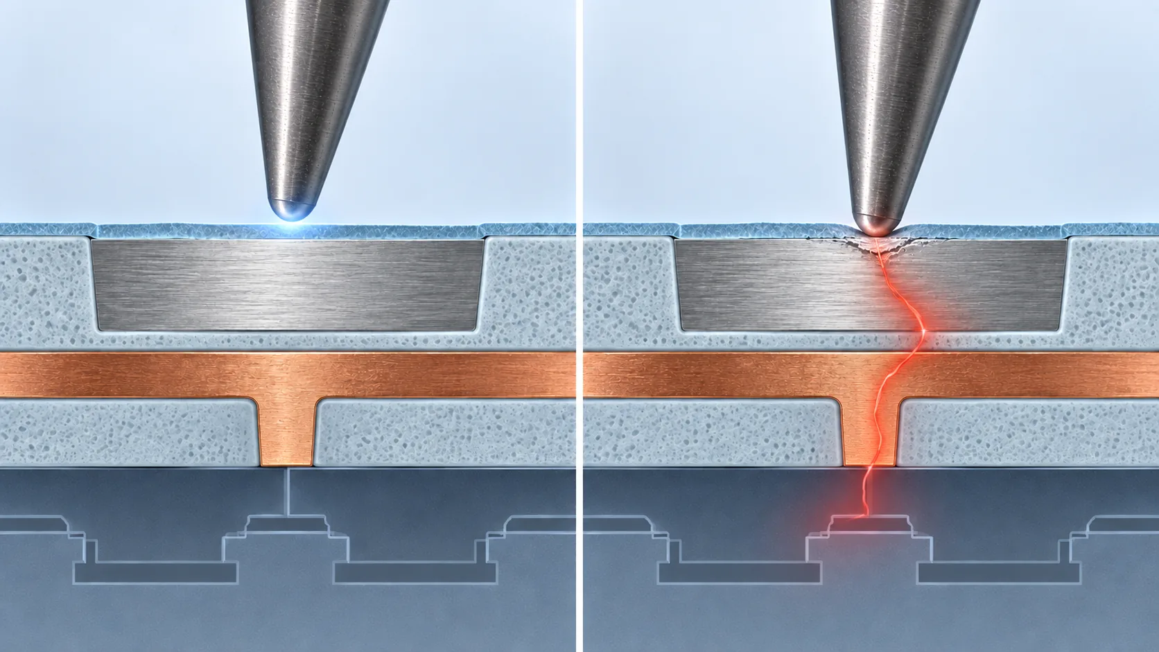
Tokyo Seimitsu's patent states that as electrode pads have grown thinner, "bringing a probe into contact with an electrode pad by the conventional method gives rise to the problem that the probe tip punches through the electrode pad film and proper contact cannot be established", and further that "the problem also arises that the electrical circuitry beneath the electrode pad is damaged and does not work correctly"Sourced.
That is where the materials-design dilemma sits.
- You want it hard: to break the oxide reliably, resist wear and survive hundreds of thousands of touchdowns
- You do not want it hard: too hard and it punches through the pad and wrecks the circuit underneath
- You want conductivity: if contact resistance rises, the measured value is wrong
- You want spring: height variation across the wafer has to be absorbed by the needle flexing
- You do not want it to foul: shaved aluminium sticks to the tip, oxidises, and resistance climbs
Hardness, conductivity, spring and wear resistance cannot all be met by one metal. When Micronics Japan advertises MEMS-V with "a high-hardness material" and "stable contact resistance" side by side, and in the same breath lists "excellent maintainability, with single-pin replacement made easy", that is a sign the card is designed on the assumption that needles are consumablesSourced. A needle is not treated as something that does not break, but as something replaced on a set schedule.
6. A materials engineer's view 2: the socket changes material part by part
Once a device is packaged, test uses a socket rather than needles. The IC drops into the socket and springs press it down onto the contacts. The one used in final test is a test socket; the one used in burn-in is a burn-in socket.
Yamaichi Electronics treats burn-in as a step with "two purposes: (1) higher reliability and (2) higher yield", and describes the job of the burn-in socket as "the contact technology that connects an IC stably to the test board"Sourced.
Here is the part that is most interesting for a materials engineer. The company lists three requirements for the contact element: "heat resistance such that characteristics do not degrade even above 150 degrees Celsius", "good conductivity" and "good fatigue properties"Sourced. And meeting all three in one material is hard. So a real socket assigns a different material to each part.
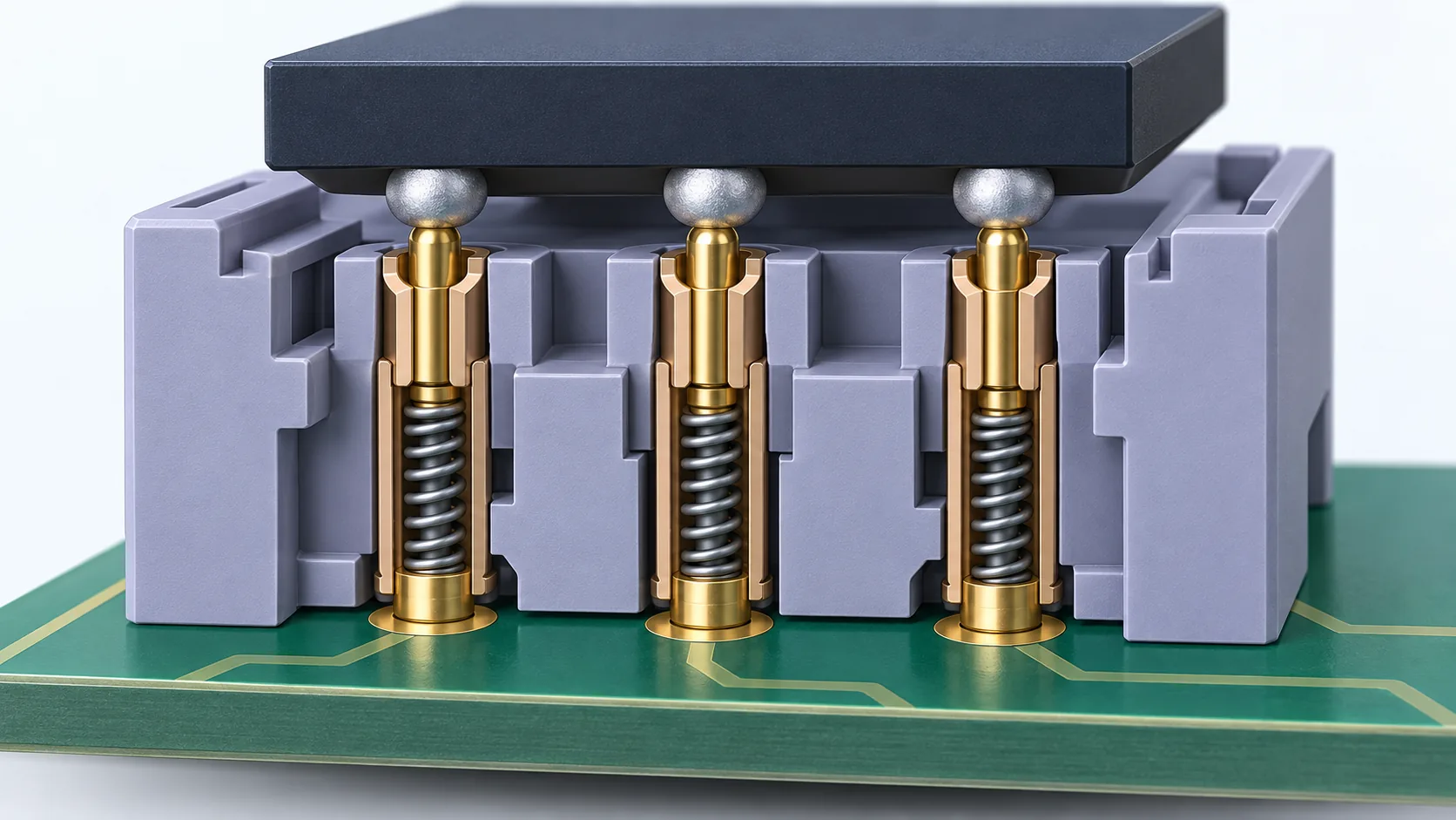
| Part | Material | What it is being asked to do |
|---|---|---|
| Housing (the body) | Super engineering plastic | Hold its shape above 150 °C. Keep the IC and the contacts in position |
| Contact (burn-in) | BeCu (beryllium copper) | Combine spring and conductivity. Survive repeated use hot |
| Contact (test) | BeCu / SK (carbon tool steel) / Pd alloy | Take a far larger number of cycles at room temperature |
| Barrel (the tube) | PB (phosphor bronze) | Guide the plunger and carry the current |
| Coil spring | SWP (piano wire) / SUS (stainless) | Generate the contact force. Do not take a set |
Material names follow Yamaichi Electronics' technical column [Source 15]. The function column is this article's own framing.
Want conductivity, reach for a copper alloy; want spring, reach for work-hardened steel; want heat resistance, reach for a resin. Instead of demanding everything from one part, split the job into functions, give each function its own part, and choose a material per part. The socket is the classic example.
For the housing, Yamaichi Electronics says it uses "super engineering plastic", with "heat resistance above 150 degrees Celsius and 1.5 times the strength of a general-purpose plastic"Sourced. What matters here is the condition that burn-in runs at 125 to 180 degrees Celsius for some hoursSourced. So the housing is required to hold its dimensions through thousands or tens of thousands of open-and-close cycles at that temperature. Heat grade selection, mould shrinkage, creep, moisture uptake: the whole list of resin-design questions lines up unchanged.
The same reading applies to the contacts. Burn-in is hot, so BeCu. Test is at room temperature but runs far more cycles, so SK (carbon tool steel) and Pd alloy join BeCu on the menuSourced. Change the temperature and the best material changes — an utterly ordinary fact, showing up directly as two different products.
7. Test in the stacking era — KGD as a precondition
Everything so far has been about measuring one chip. But the back end is now moving in the direction of stacking chips (see the HBM, Stacking and Hybrid Bonding articles). Seen from the test side, stacking has an awkward property.
Once it is stacked, you cannot pull one layer back out.
So you need dice that are already known to be good before you stack them. That is KGD (known good die). Texas Instruments states that "KGD is defined as a die with the same quality and reliability as an equivalent packaged component"Sourced. A KGD, in other words, is a bare die that carries the same quality assurance as a packaged part despite not being in a package.
Tokyo Electron likewise says that in the wafer test step "securing KGD is important"Sourced. Which is to say the weight of wafer test is shifting from "drop the bad ones early" to "issue the quality assurance that stacking depends on".
Test used to be the last gate, there to stop bad parts getting out. With stacking the meaning changes. Mix in a single bad die and it drags the good dies stacked with it down too. If one layer of a 16-high stack is bad, what gets scrapped is the whole stack, including the fifteen good dies in it.
So test moves forward from the back of the flow to an earlier stage. The point raised in the Stacking article, that the benefit of stacking evaporates unless good and bad are known beforehand, is, seen from the test side, exactly the same thing as the bar for KGD going up.
What has changed for the people measuring stacked memory
Advantest's memory test handler M5241 is described as "optimised for volume testing of DRAM, NAND flash and HBM", with up to 512 devices measured in parallel, a temperature range of −40 to +125 °C as standard (−55 to +150 °C extended), "±1.0 °C accuracy achieved by a micro-chamber approach", a maximum throughput of 46,000 UPH and a maximum device size of 14 × 22 mmSourced.
On the tester side, the company announced T5801 for next-generation DRAM on 12 February 2025. It claims "industry-leading performance of up to 36 Gbps PAM3 and 18 Gbps NRZ", and gives as the background that "memory bandwidth is becoming a potential bottleneck in overall system performance"Sourced. Sales are planned to start in early 2026Not yet confirmed.
Memory getting faster means the tester has to be able to send and receive signals at that speed too. A number like 36 Gbps is a requirement placed on the measuring instrument. And that signal reaches the device through the wiring of a socket or a probe card. Once high-speed signals pass through it, the dielectric properties (Dk and Df) of the board material used there start to matter. The low-Df argument from the Build-up Film article applies not only to the board in the product but to the test fixture, for exactly the same reason (Commentary).
8. What is still hard
(1) Test sells time — which is why it measures in parallel
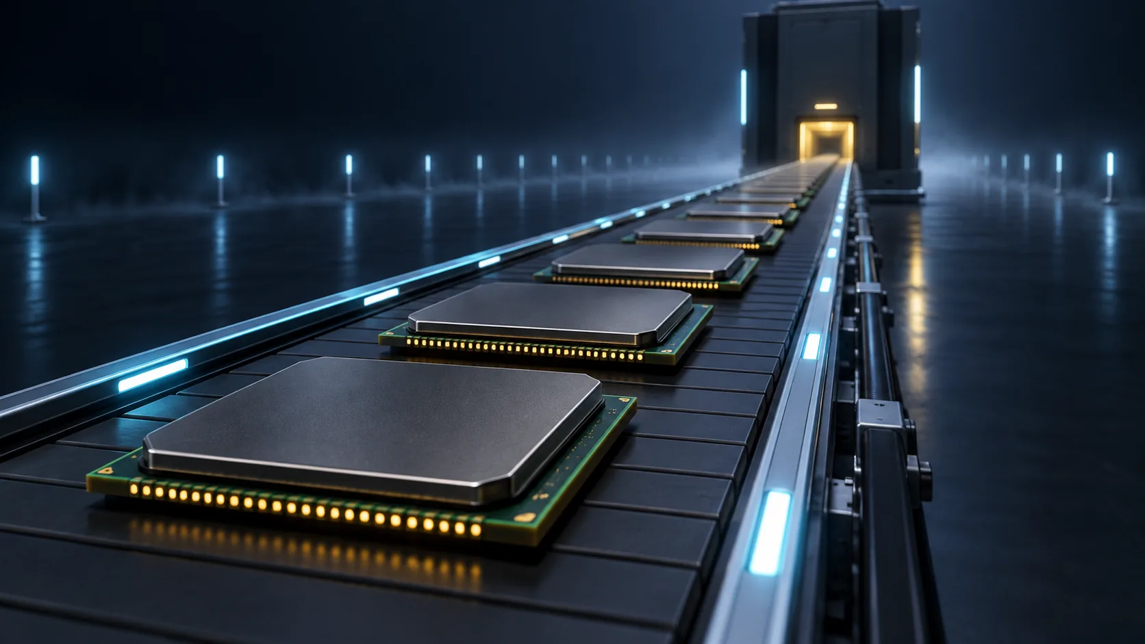
Boiled down, the cost of test is set by how many seconds you occupied the machine. The more complex the chip, the more items there are to confirm, and the longer each part takes. There is only one way to absorb that: measure many of them at once.
Advantest's SLT and burn-in platform 7038 is described as able to "measure up to 720 devices in parallel and deliver a throughput of 5,000 units per hour (UPH)", and as offering "customisable test specifications such as voltage, temperature and burn-in time"Sourced.
Measuring 720 devices at once needs 720 sockets. A handler running 512 in parallel has 512 sockets sitting on the board. A probe card for 2,500 DUT stands about 200,000 needles on a single boardSourced.
So the industry's push to raise the parallel count converts directly into demand for contact materials, resins and boards. And these are consumables. Needles, springs and contacts all reach end of life after a set number of cycles. Win the design in once and the orders keep coming — a distinctly unusual characteristic even among back-end materials (Commentary).
(2) Measuring while getting the heat out
A chip under test generates heat, and the more power-hungry the device, as with AI parts, the more heat it makes. Change the temperature and the characteristics change, and the verdict wobbles with them.
Tokyo Electron citing "heat-absorption control for high heat generation" on its proberSourced, and Advantest stating "±1.0 °C accuracy achieved by a micro-chamber approach" on its handlerSourced, are both saying the same thing: holding temperature at a set value while you measure is a precondition of the measurement itself.
That is a materials and structures problem. How to take the heat, how to move it out, how to keep it uniform — the TIM (thermal interface material) and heat-spreading arguments from the HBM and CoWoS articles exist in the same form on the test-fixture side (Commentary).
(3) Pads are getting thinner — touching them is getting harder
On thinning electrode pads, Tokyo Seimitsu's patent raises the problems that "the probe tip punches through the electrode pad film and proper contact cannot be established" and that "the electrical circuitry beneath the electrode pad is damaged and does not work correctly"Sourced.
The further scaling goes, the narrower the window of acceptable penetration depth becomes. Too shallow and the oxide is not broken; too deep and the circuit is destroyed. The conversation about needle material and shape connects here, directly, to the wiring and dielectric design on the process side.
(4) Failures remain that ATE cannot catch
Advantest gives as the background to SLT "market demands such as testing increasingly complex devices, cutting test cost, and large-scale volume production"Sourced. However carefully test patterns are built, they cannot fully reproduce a state in which an OS is running, several chips are working at once and the supply rail is moving. So one more stage, SLT, is stacked on top — meaning the number of test stages is itself growing.
Test looks like the least glamorous step in the whole back end. But as this article has shown, what is inside it is the materials engineering of contact (needles, contacts, plating, wear), structural materials (a board that will not flex under a tonne, a resin that holds its dimensions at 150 °C), thermal design (holding temperature during measurement), and the economics of yield (when to throw a part away), all acting at once.
Seen from a materials supplier, test tooling is a low-volume, high-unit-price, repeat-order market, unusual even among back-end materials. And with stacking and the growth of AI silicon, the volume is heading up (Commentary).
9. Glossary
- Wafer test
- The step that judges each chip electrically before the wafer is cut apart. Also called wafer probing or wafer sort.
- Final test
- The step that confirms a device works correctly as a finished part after it has been packaged.
- Burn-in
- A test that applies heat and voltage to bring early-life failures out sooner so they can be screened away.
- SLT
- System level test. Running an OS and software for verification in an environment close to the end product.
- ATE
- Automated test equipment. The tester itself plus the handling equipment around it.
- Test head
- The part holding the boards that carry the test functions. Placed right next to the device being measured.
- Prober
- The machine that carries the wafer, aligns it and brings it into contact with the probe card.
- Test handler
- The machine that carries packaged devices and loads them into sockets.
- Probe card
- The fixture joining chip electrodes to the tester: many needles (probes) arranged on a wiring board.
- DUT
- Device under test. Also used as the unit for how many parts are measured in parallel.
- Overdrive
- How far the needle is pushed in beyond first touching the pad. Needed to break the oxide, damaging in excess.
- Scrub mark
- The scar the needle leaves as it slides across the pad surface. Evidence of contact, and something to be controlled.
- KGD
- Known good die. A bare die guaranteed to the same quality and reliability as a packaged part.
- UPH
- Units per hour. The number of parts processed per hour, a measure of test equipment throughput.
- BeCu
- Beryllium copper. A copper alloy that is both conductive and springy. Widely used for contacts.
- Super engineering plastic
- The general term for high-performance resins with excellent heat resistance and strength. Used for socket housings.
10. Primary sources
- Advantest "Business introduction (explainer: semiconductor test)" (Japanese-language page) — advantest.com
- Advantest "What is ATE (automated test equipment)?" (Japanese-language page) — advantest.com
- Advantest "System level test systems" (Japanese-language page) — advantest.com
- Advantest "7038 massively parallel system level test (SLT) and burn-in (BI) platform" (Japanese-language page) — advantest.com
- Advantest "Advantest announces T5801, an ultra-high-speed memory test system for next-generation DRAM", 12 February 2025 (Japanese-language page) — advantest.com
- Advantest "M5241 test handler" (Japanese-language page) — advantest.com
- Tokyo Electron "Test: Prexa series" (Japanese-language page) — tel.co.jp
- Micronics Japan "Probe cards" (Japanese-language page) — mjc.co.jp
- Micronics Japan "U-Probe" (Japanese-language page) — mjc.co.jp
- Micronics Japan "MEMS-V" (Japanese-language page) — mjc.co.jp
- Japan Electronic Materials "Components for semiconductor inspection" (Japanese-language page) — jem-net.co.jp
- Japan Electronic Materials "Probe cards" (Japanese-language page) — jem-net.co.jp
- Tokyo Seimitsu (published patent) "Prober, probe contact method and program therefor", JP4817830B2 (Japanese-language page) — patents.google.com
- Yamaichi Electronics "What materials and technologies go into burn-in and test sockets for semiconductor inspection? Part 1" (Japanese-language page) — yamaichi.co.jp
- Yamaichi Electronics "What materials and technologies go into burn-in and test sockets for semiconductor inspection? Part 2" (Japanese-language page) — yamaichi.co.jp
- Yamaichi Electronics "What is a burn-in socket? The IC socket for inspection that supports our comfortable lives" (Japanese-language page) — yamaichi.co.jp
- Texas Instruments "Die and wafer solutions" (Japanese-language page) — tij.co.jp
11. Claim-to-source audit
| Claim in the text | Basis | Label |
|---|---|---|
| That test "compares the output waveform of a semiconductor against a reference and judges it good or defective"; that test systems are "used at the end of the wafer fabrication process, and again at final inspection after packaging and the rest"; that what is looked at is "whether the semiconductor operates properly, and whether it meets the performance and endurance being asked of it"; that the aim includes "analysing the cause of failures and raising yield"; and the make-up of a test system (test head, handling equipment meaning prober or test handler, and device interface) | Advantest "Business introduction (explainer: semiconductor test)"[Source 1] https://www.advantest.com/ja/about/business/ | Sourced |
| That wafer-level test is "testing carried out at the stage before the wafer is divided into individual dice" which "checks the electrical characteristics of each die on the wafer and helps find defects early"; that package test is "a test that confirms a packaged device operates correctly as a finished semiconductor device" and "verifies that it operates stably under conditions such as temperature change"; and that SLT is "a test that runs an OS and software for verification on a platform reproducing operating conditions close to the real use environment of an end product such as a smartphone or a PC" | Advantest "What is ATE?"[Source 2] https://www.advantest.com/ja/semiconductor-basics/automated-test-equipment/ | Sourced |
| That SLT "tests the behaviour of a semiconductor in the real use environment where it is built into a system or an end product", and that behind it lie "market demands such as testing increasingly complex devices, cutting test cost, and large-scale volume production" | Advantest "System level test systems"[Source 3] https://www.advantest.com/ja/products/component-test-system/system-level-test-systems/ | Sourced |
| That the 7038 can "measure up to 720 devices in parallel and deliver a throughput of 5,000 units per hour (UPH)", and that "test specifications such as voltage, temperature and burn-in time are customisable" | Advantest 7038 product page[Source 4] https://www.advantest.com/ja/products/component-test-system/system-level-test-systems/7038/ | Sourced |
| That T5801 was announced on 12 February 2025; that it claims "industry-leading performance of up to 36 Gbps PAM3 and 18 Gbps NRZ"; and that the company states "memory bandwidth is becoming a potential bottleneck in overall system performance" | Advantest news release, 12 February 2025[Source 5] https://www.advantest.com/ja/news/2025/20250212.html | Sourced |
| That sales of T5801 are planned to begin in early 2026 (no shipment record confirmed as this article was written) | Advantest news release, 12 February 2025[Source 5] https://www.advantest.com/ja/news/2025/20250212.html | Not yet confirmed |
| That the M5241 is "optimised for volume testing of DRAM, NAND flash and HBM"; up to 512 devices in parallel; a temperature range of −40 to +125 °C (extended −55 to +150 °C); "±1.0 °C accuracy achieved by a micro-chamber approach"; up to 46,000 UPH; and a maximum device size of 14 × 22 mm | Advantest M5241 product page[Source 6] https://www.advantest.com/ja/products/component-test-system/test-handler/m5241/ | Sourced |
| That Prexa MS is a fully automatic 300 mm wafer prober; that "the test pin count and the heat generated are both increasing"; that it "handles an ultra-high load capacity of up to 1000 kg"; that it "enables full-wafer test (single-touchdown contact) for coming memory devices"; that it has "heat-absorption control for high heat generation"; XY ±0.8 µm and Z ±2.5 µm (option ±5.0 µm); and that in the wafer test step "securing KGD is important" | Tokyo Electron "Test: Prexa series"[Source 7] https://www.tel.co.jp/product/prexa.html | Sourced |
| That a probe card is "a tool used for the electrical inspection of LSI chips formed on a silicon wafer, in the wafer inspection step of LSI manufacture", that it "is fitted to a wafer prober and acts rather like a connector joining the electrodes of the LSI chip to the LSI tester that does the measuring", and that "the needles of the probe card are brought into contact with the electrodes of the LSI chip, electrical inspection is carried out, and a good/bad judgement is made" | Micronics Japan "Probe cards"[Source 8] https://www.mjc.co.jp/products_service/probecard/ | Sourced |
| That U-Probe is "a probe card for massively parallel measurement of DRAM and flash memory devices"; that it "supports about 2,500 DUT and about 200,000 probe pins on a single card"; that it "also handles single-touchdown measurement of a 12-inch wafer"; and that it rests on "our own MEMS probe, the micro-cantilever, together with our thin-film multilayer wiring board manufacturing technology" | Micronics Japan "U-Probe"[Source 9] https://www.mjc.co.jp/products_service/probecard/u_probe/ | Sourced |
| That MEMS-V is a "square needle type" probe card using "a new MEMS probe in a high-hardness material, wear-resistant and long-lived", with "high probe positional accuracy and stable contact resistance", "excellent maintainability, with single-pin replacement made easy", "capability for high- and low-temperature testing over a large probing area", and support for fine-pitch devices | Micronics Japan "MEMS-V"[Source 10] https://www.mjc.co.jp/products_service/probecard/mems_v/ | Sourced |
| That wafer test "decides whether the IC chips that have been made are good or defective, before the hundreds of IC chips laid out on the wafer are cut (diced) into chips a few millimetres square" | Japan Electronic Materials "Components for semiconductor inspection"[Source 11] https://www.jem-net.co.jp/products/handotai | Sourced |
| That probe cards are classified into M type (MEMS), V type (vertical) and C type (cantilever); that the MC series is "used mainly for wafer test of DRAM and NAND flash memory" and "carries the most probes of any of our products"; that the MT series "handles fine-pitch area-array layouts and is ideal for measuring flip chips"; and that the CE series is "widely used across various fields, centred on logic ICs" | Japan Electronic Materials "Probe cards"[Source 12] https://www.jem-net.co.jp/products/probe | Sourced |
| That "when the number of probes making contact changes, the total contact pressure taken by the probe card as a whole changes accordingly, and with it the amount by which the probe card deflects"; that "such changes in contact pressure were not particularly taken into account, being regarded as small in effect"; and the problems that "the probe tip punches through the electrode pad film and proper contact cannot be established" and "the electrical circuitry beneath the electrode pad is damaged and does not work correctly" | Background art of Tokyo Seimitsu's published patent JP4817830B2[Source 13] https://patents.google.com/patent/JP4817830B2/ja | Sourced |
| That socket housings use "super engineering plastic", with "heat resistance above 150 degrees Celsius and 1.5 times the strength of a general-purpose plastic", and that injection moulding and machining are both used | Yamaichi Electronics technical column Part 1[Source 14] https://www.yamaichi.co.jp/column/howtomake_part1/ | Sourced |
| That contact materials are BeCu (beryllium copper) in burn-in sockets, and BeCu, SK (carbon tool steel) or Pd alloy in test sockets; that barrels are PB (phosphor bronze) and coil springs SWP (piano wire) or SUS (stainless); and that the requirements are "heat resistance such that characteristics do not degrade even above 150 degrees Celsius", "good conductivity" and "good fatigue properties" | Yamaichi Electronics technical column Part 2[Source 15] https://www.yamaichi.co.jp/column/howtomake_part2/ | Sourced |
| That burn-in is "the temperature-and-voltage test carried out at the final stage of semiconductor manufacturing", which "stresses parts with temperature and voltage for some hours in a high-temperature environment of 125 to 180 degrees Celsius, to screen out early-life failures"; that its purpose is "two things: (1) higher reliability and (2) higher yield"; and that the burn-in socket provides "the contact technology that connects an IC stably to the test board" | Yamaichi Electronics technical column "What is a burn-in socket?"[Source 16] https://www.yamaichi.co.jp/column/what-is-a-burn-in-socket-an-ic-socket-for-inspection-use-that-supports-our-comfortable-lives/ | Sourced |
| That "KGD is defined as a die with the same quality and reliability as an equivalent packaged component" | Texas Instruments "Die and wafer solutions"[Source 17] https://www.tij.co.jp/ww/hirel/die/index.shtml | Sourced |
| Fig. 4: the estimate of about 5 gf of contact force per needle, back-calculated from Tokyo Electron's "up to 1000 kg" and Micronics Japan's "about 200,000 pins". These are separate products from separate companies and the figure does not describe any real machine combining the two | Our calculation, worked backwards. The underlying numbers come from Sources 7 and 9[Source 7] https://www.tel.co.jp/product/prexa.html[Source 9] https://www.mjc.co.jp/products_service/probecard/u_probe/ | Our calculation |
| Fig. 8: stack yield taken as pn for a per-layer yield p and n layers (4, 8, 12 and 16 layers at 99%, 98% and 95%) | A simple calculation by this article, not measured values for any product. Redundancy, repair and post-stack rescue mean reality does not follow it exactly | Our calculation |
| The framing that the properties asked of a needle (hardness, conductivity, spring, wear resistance, freedom from pick-up) contradict one another; the reading that the socket is an example of splitting a job into functions; the point that a rising parallel count converts directly into volume of contact material, resin and board; the point that test tooling has the market character of low volume, high unit price and repeat orders; and the point that Dk/Df and heat removal for high-speed signals matter in inspection fixtures too | Commentary and framing by this article, built on published material. Not a view expressed by any of the companies, nor an established industry classification | Commentary |
| That the three numbers placed side by side in Fig. 10 (about 2,500 DUT, 512 devices, 720 devices) cover different process steps measuring different things and cannot be compared as a ranking | Our note in this article. The figures themselves come from Sources 4, 6 and 9[Source 4] https://www.advantest.com/ja/products/component-test-system/system-level-test-systems/7038/[Source 6] https://www.advantest.com/ja/products/component-test-system/test-handler/m5241/[Source 9] https://www.mjc.co.jp/products_service/probecard/u_probe/ | Commentary |
Last updated 20 September 2026. Sources are limited to primary material (official product pages and news releases from equipment and fixture makers, a published patent, and a device maker's official technical page). Because the article contains process framing and readings about materials design, those passages are marked Commentary to separate them from sourced fact. All figures are explanatory concept graphics. Visual-overview figures are shown as AI-generated conceptual images, matching the Japanese edition. Vector drawings are retained where they carry quantitative values or precision-critical technical labels. AI-generated images do not depict real equipment, products, facilities, dimensions or exact cross-sections; replaced source SVG overview drawings remain in the HTML but are hidden.