TECHNOLOGY EXPLAINER
What a Package Substrate Is
— the converter that bridges a millionfold gap between nanometres and millimetres
Almost every conversation about semiconductors is about what happens inside the silicon. In the AI era, though, the bottleneck is often outside it — in the board the chip sits on. This is a field where materials engineering takes the lead role, explained from the beginning.
- What a package substrate is (the short version)
- Why it is needed — a millionfold change of scale
- Structure: the core layer and the build-up layers
- How the wiring gets made (the SAP process)
- A materials engineer's view: ABF and five demands that fight each other
- The battle over core material — holding warpage down
- Why this became a bottleneck now
- Glass cores as the next move
- What is still hard
- Glossary / Primary sources / Claim-to-source audit
Sourced = a value stated in published material from a device or materials manufacturer (link given)
Our calculation = a figure this article derived, with the assumptions spelled out
Not yet confirmed = work in development or under study, with no confirmed production record
1. What a package substrate is (the short version)
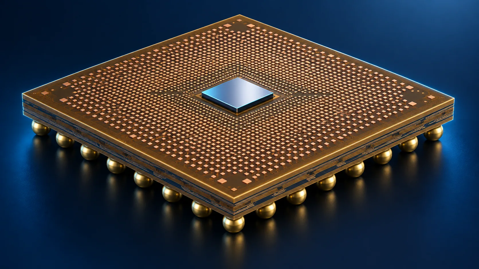
A package substrate (IC substrate, or FC-BGA substrate) is a multilayer wiring board that carries a silicon chip and converts its extremely fine terminals into terminals a motherboard can handle.
- Carry: support the silicon die mechanically and protect it
- Connect: route the die's thousands to tens of thousands of terminals through internal wiring layers
- Convert: fan micrometre-scale terminals out to millimetre-scale solder balls
An Intel packaging engineer puts the role bluntly: "a substrate is essentially a space transformer"Sourced. The silicon die holds circuitry at nanometre scale and gathers it into micrometre-scale pads on its underside; the substrate converts that into the millimetre-scale connections the motherboard uses (Intel, November 2023).
2. Why it is needed — a millionfold change of scale
"Why not mount the chip straight onto the motherboard?" is usually the first question. The answer is that the dimensions are too far apart.
The gap between a nanometre and a millimetre is a factor of a millionOur calculation. You cannot clear that in a single jump. So an intermediate board that can handle micrometre-scale wiring goes in between, and the fan-out happens in stages. A package substrate is the dedicated converter for exactly that.
And in AI silicon, the demands on that converter have sharpened abruptly. Terminal counts have gone from thousands to tens of thousands, signalling has got faster, package dimensions have grown. The converter's performance has started to limit the chip's performance — which is the subject of this article.
3. Structure: the core layer and the build-up layers
A package substrate is, broadly, made of two parts.
The core layer — strength as a board
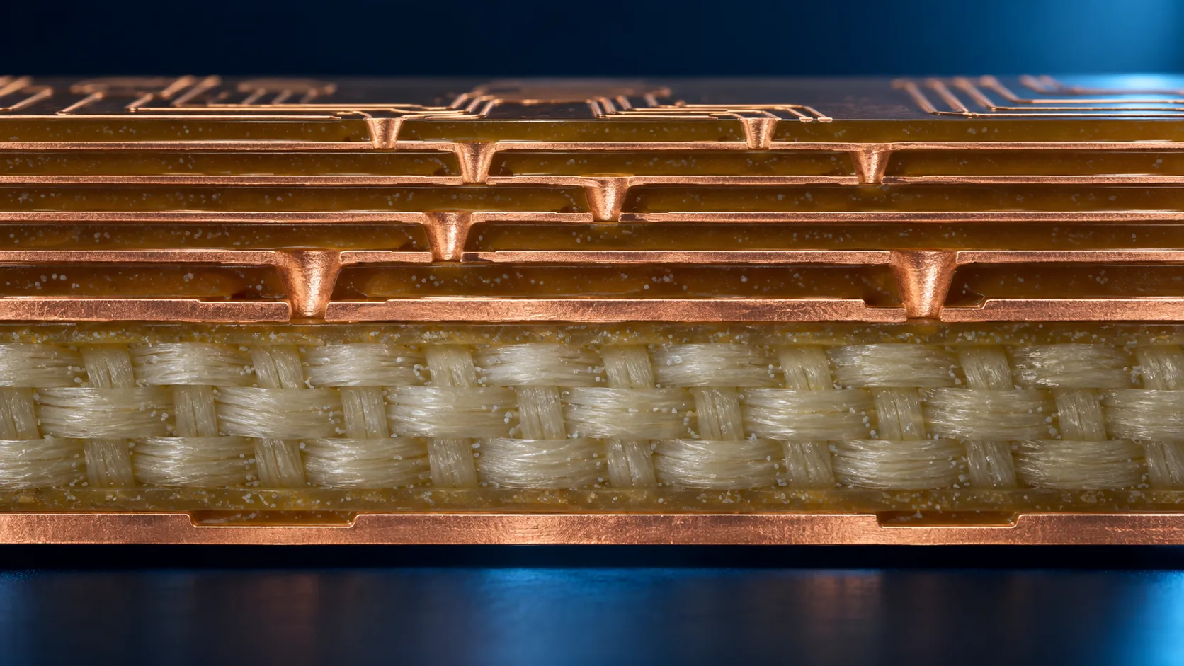
The thicker layer in the middle, made of glass cloth impregnated with resin. It provides the substrate's stiffness and flatness and connects front to back through plated through-holes. Let this get weak and the board warps under heat.
The build-up layers — fineness of wiring
Above and below the core, dielectric layers and copper wiring layers alternate. The dielectric is a film-form material, of which ABF (Ajinomoto Build-up Film) is the archetype; Ajinomoto gives the thickness as roughly 10 µm per layerSourced (Ajinomoto). Layer-to-layer connections are made by tiny holes called microvias.
4. How the wiring gets made (the SAP process)
There are broadly two ways to make fine copper traces: etch away a sheet of copper and keep what is left (subtractive), or grow copper only where it is wanted (additive).
For fine wiring the mainstream is the second: SAP, the semi-additive process. Ibiden states that its conductor formation technology, centred on SAP, achieves world-class fine wiringSourced (Ibiden).
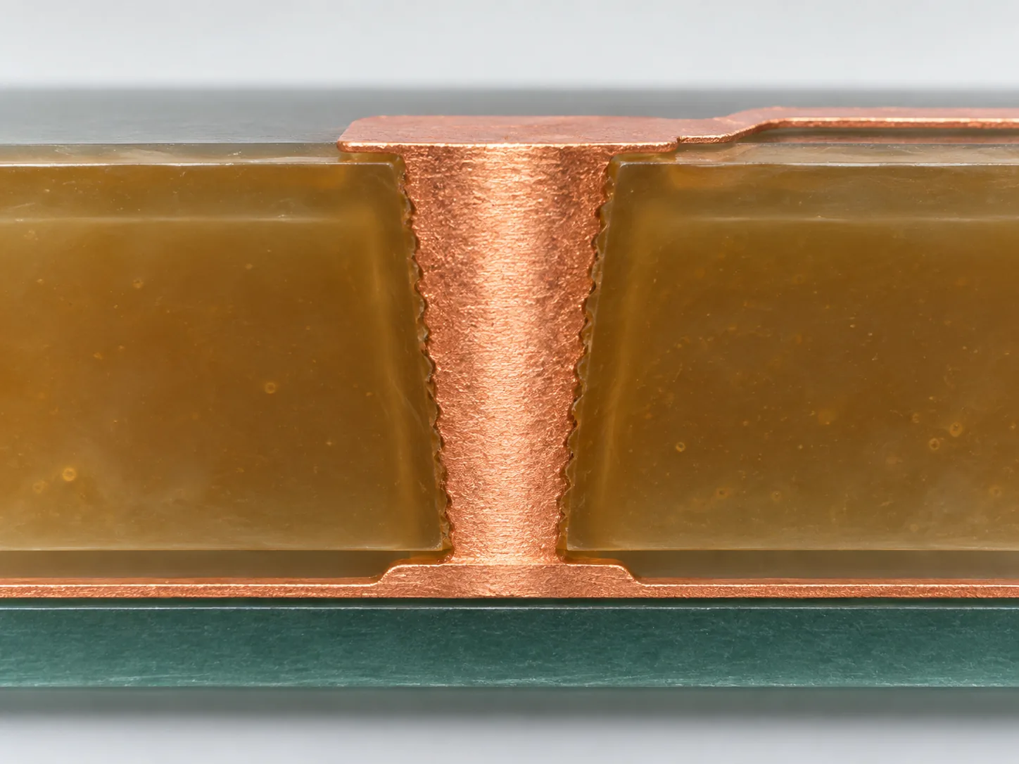
Ajinomoto says of ABF that "micrometre-scale electronic circuitry can be formed by laser processing and by plating copper directly onto the surface"Sourced (Ajinomoto). The dielectric, in other words, is designed together with the way it will be processed.
5. A materials engineer's view: ABF and five demands that fight each other
ABF — a de facto standard that came out of Japan
As the dielectric for build-up layers, ABF (Ajinomoto Build-up Film) has become the de facto standard.
| Item | What Ajinomoto states |
|---|---|
| Launched | 1999 |
| Share | "About 95%" (story page) / "close to 100% of leading personal computers" (innovation story) |
| Composition | A formulation combining epoxy resin, curing agent, inorganic filler and flame retardant |
| Thickness | About 10 µm per layer |
| Processing | Micrometre-scale circuitry formed by laser processing and direct copper plating on the surface |
| Why it became a film | The older liquid ink suffered from uneven coating, bubbles and harmful gas. A film only has to be laminated, which shortens the process |
All Sourced (Ajinomoto published material, Japanese-language pages). The company words the share differently on two of its pages, so both are given.
A food company holding an overwhelming share of a semiconductor material is an interesting fact in itself. What matters technically, though, is that the demands placed on this material contradict one another.
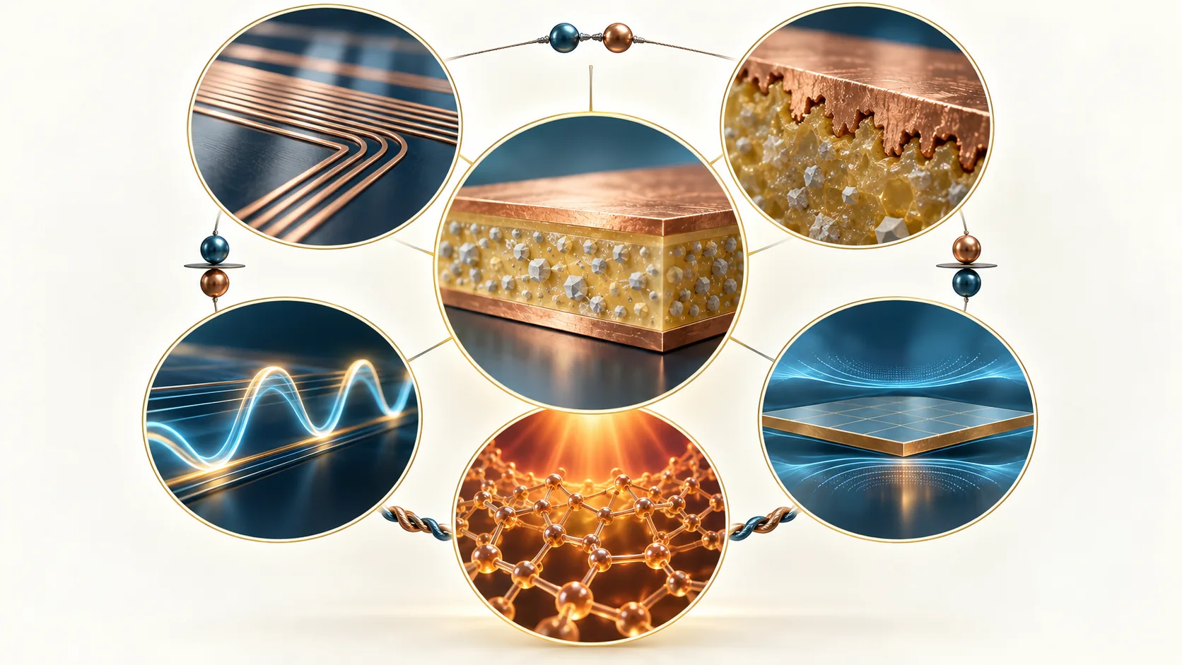
Clash 1: smoothness against adhesion
The surest way to make plated copper stick is to roughen the surface so the copper keys into the resin, an anchor effect.
But once traces get fine, that same texture ruins their edges and invites opens and shorts.
At high frequency the texture becomes transmission loss in its own right. The finer you go the smoother you want it, and the smoother it gets the more it peels.
Clash 2: low permittivity against heat resistance and adhesion
Lowering Dk and Df means suppressing molecular polarity and opening up free volume.
That direction generally works against heat resistance and adhesion.
Clash 3: low thermal expansion against processability
Suppressing warpage calls for more inorganic filler to bring expansion down.
But more filler costs you laser processability and the flexibility the film needs.
And to make traces finer, the filler particles themselves have to get finer too.
Making all five work at once is what developing a package substrate dielectric actually is. Building a material that excels at any one of them is not hard. Landing all of them on an acceptable compromise is.
6. The battle over core material — holding warpage down
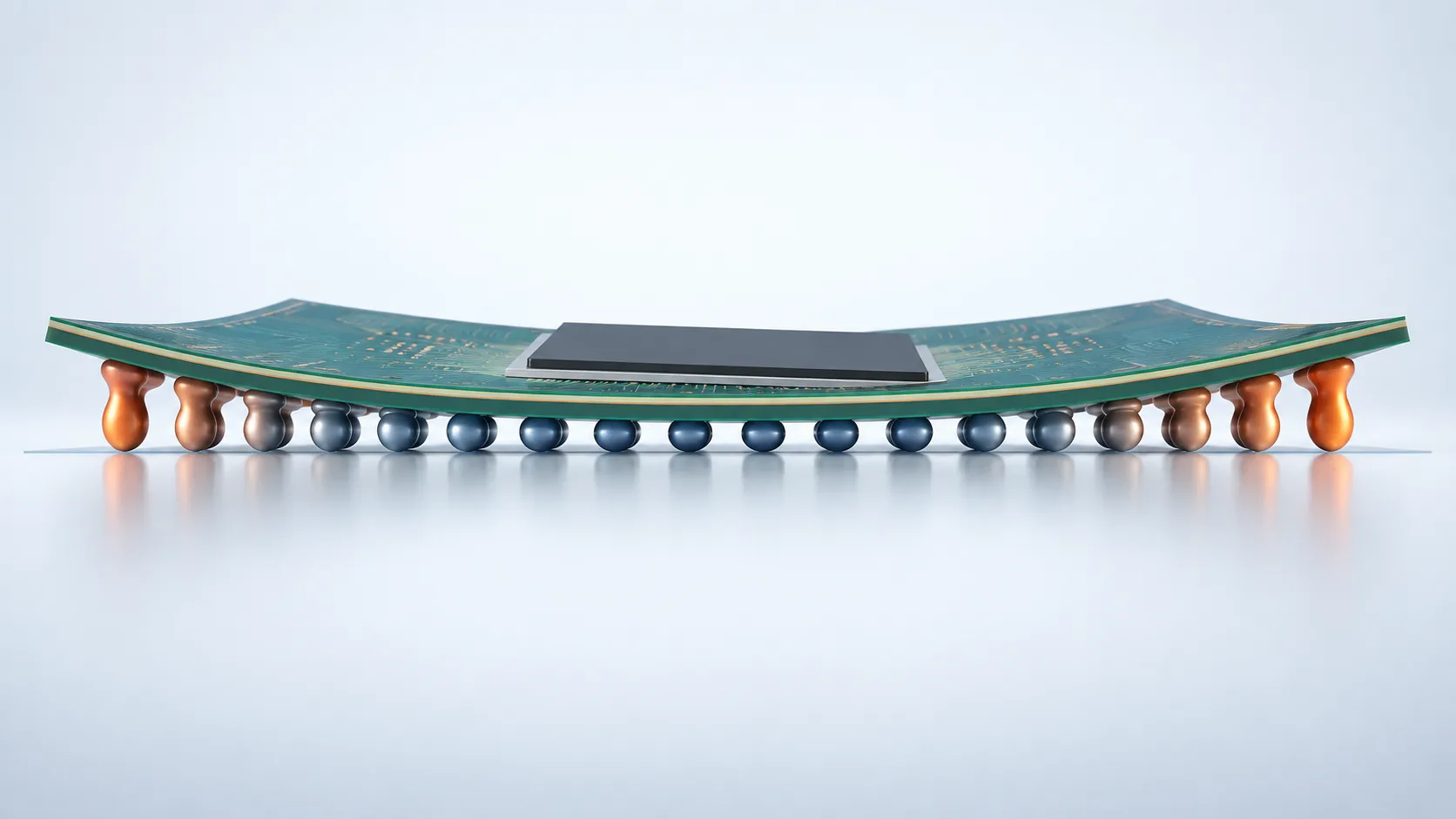
Where the build-up layers deliver fineness of wiring, the core layer decides how the thing behaves as a board. And as AI packages have grown, this has become a serious problem.
Resonac's low-expansion copper-clad laminate
On 12 February 2025, Resonac announced that it had developed a low-thermal-expansion copper-clad laminate (CCL) to suppress the warpage that comes with larger semiconductor packagesSourced. What was published is as follows (Resonac).
| Item | What Resonac states |
|---|---|
| Aim | Suppressing the warpage that accompanies larger packages |
| Target size | Semiconductor packages larger than 100 mm × 100 mm |
| Result | Four times the durability of the conventional product in thermal cycling tests |
| Development method | Multiscale analysis (computational science) used to make the design guidance for each constituent material explicit |
| Materials design | Lower the coefficient of thermal expansion to suppress warpage, and lower the elastic modulus to suppress cracking on cooling |
| Production | Targeting 2026 |
| Organisation | 70% of computational and information science research resources allocated to semiconductor materials development |
All Sourced (Resonac news release, 12 February 2025, Japanese-language release).
The striking part is that it targets lower thermal expansion and lower elastic modulus at the same time. Intuition says a stiffer board warps less. But a material that is too stiff cannot shed the contraction stress of cooling, and it cracks. Resisting warpage and resisting cracking often pull in opposite directions.
More important still, that optimum was narrowed down by multiscale analysis before any experiment. Above 100 mm square, a single prototype costs a great deal in money and time. The decisive ground in materials development is shifting from trial-and-error formulation toward design by computation — which is how it reads alongside the statement about 70% of research resources going to semiconductor materials.
7. Why this became a bottleneck now
The package substrate was treated as an unremarkable component for a long time. The reason it now draws attention on both supply and technology is that AI requirements are advancing in three directions at once.
| Direction | What is happening | Effect on materials |
|---|---|---|
| 1. Larger formats | Chiplets and on-package HBM enlarge the package area | Warpage worsens with size. Over 100 mm square has to be handled |
| 2. More layers, finer wiring | More layers and finer traces to serve rising terminal counts | The thinner the layer, the narrower the flatness budget |
| 3. Higher speed | Signalling rates climb | Dielectric loss and surface roughness turn directly into transmission loss |
AT&S puts the situation plainly: "As packages become larger and dielectric layers thinner, the tolerance for flatness narrows. Warpage control, not only at room temperature but through reflow and thermal cycling, becomes a central factor in reliability and yield"Sourced (AT&S).
The new failure modes that fine geometry brings
The same company notes that as dimensions shrink, reliability risks that used to be minor turn into the rate-limiting factorSourced.
1. Copper fatigue at interfaces
2. Voiding in via fills
3. The risk of conductive anodic filament (CAF) formation
And these, it says, "grow unless chemistry, plating profiles and dielectric selection are precisely controlled". Note that the discussion is framed as a matter of materials and chemistry, not of equipment or design.
CAF is the phenomenon where copper grows dendritically along the fibres of the glass cloth and shorts between traces. It gets more likely as trace spacing narrows, so the adhesion between glass cloth and resin in the core, and the core's moisture uptake, bear on it directly. Higher density raises the demands on the core material: that is the chain of consequence here.
UHDI, the next level
AT&S calls the next-generation target UHDI (Ultra-High-Density Interconnect) and defines it as followsSourced.
- Achieving single-digit micrometre line and space in the build-up layers
- Placing microvia structures scaled down to a few tens of micrometres in diameter
- Supporting bump and ball pitches below 100 µm, suited to multi-die and chiplet configurations
8. Glass cores as the next move
Improvement along the organic line is starting to show its limits. That has brought replacing the core layer with glass into serious play.
AT&S holds that conventional organic laminates are running into limits on three fronts: warpage, line and space scaling, and dielectric loss, and describes the advantages of glass as followsSourced (AT&S).
| Property of glass | What it delivers |
|---|---|
| CTE can be designed close to that of silicon | Lower thermomechanical stress and warpage during assembly and thermal cycling |
| Extremely low TTV (total thickness variation) | Very low warpage, favouring lithography and fine bump formation |
| High resistivity and low loss tangent | Signal quality maintained from GHz into millimetre wave, with reduced parasitics |
| Can be formed in large panels | Unlike silicon interposers, it fits advanced assembly lines |
| Optical transparency, low surface roughness, dimensional stability | Suited to co-packaged optics |
Structurally, TGVs (through-glass vias) carry the vertical power and signal paths. Metallisation comes either as full copper fill or as sidewall plating with a dielectric fill, and the two are said to carry different trade-offs in stress and reliabilitySourced.
Intel also announced glass substrates in September 2023, citing the potential for ten times the interconnect density, a 50% reduction in pattern distortion, and a dramatic reduction in the warpage problem that constrains organic substratesSourced. Market introduction is planned for the latter half of this decade.
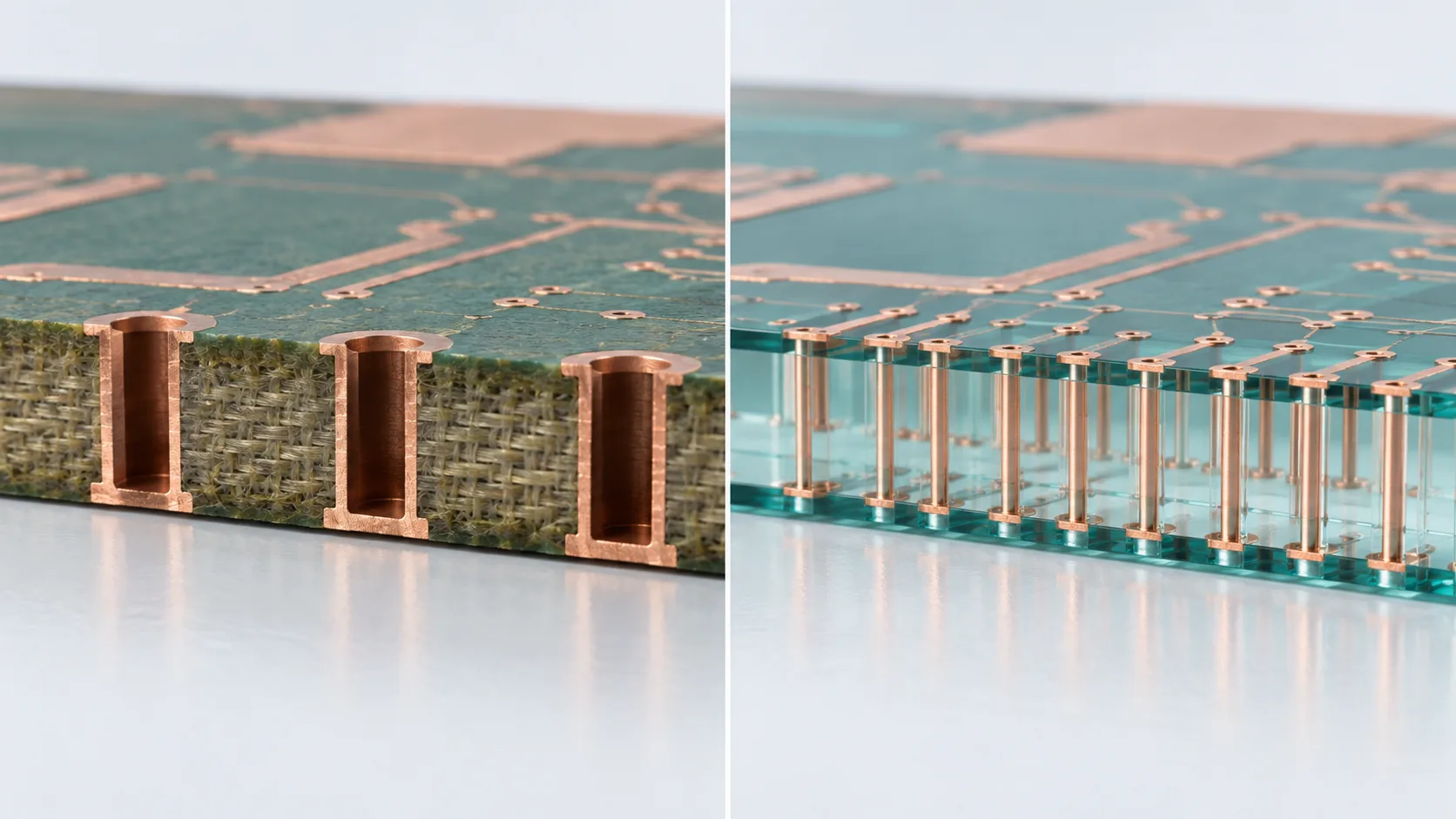
Production timing, yield and cost for glass core substrates were not published as of this article's researchNot yet confirmed. AT&S describes itself as at the stage of collaborating with semiconductor makers on prototype development, and Intel says the latter half of this decade. It matters not to confuse a roadmap target with a production record. Glass also brings problems of its own: it is prone to edge cracking and it is hard to cut.
9. What is still hard
(1) Concentration of supply
ABF is a material for which Ajinomoto publishes a share of "about 95%" up to "close to 100% of leading personal computers"Sourced. A structure in which a critical material sits with one supplier is efficient in normal times and can become a supply constraint when demand spikes.
(2) Warpage and thermal cycling
As Sections 6 and 7 showed. Larger packages translate directly into worse warpage. Resonac naming packages above 100 mm square explicitly is a sign that this level has become a real requirement.
(3) Fine geometry together with reliability
Copper fatigue, voids in vias, CAF. All of them surface as wiring gets finer and denser. The direction that raises performance and the direction that preserves reliability are in head-on conflict, and that is what makes this area hard.
10. Glossary
- Package substrate
- The multilayer board that carries a silicon die and converts its terminals to motherboard scale. Also called an IC substrate.
- FC-BGA
- Flip Chip Ball Grid Array. A package style where the die is flipped and joined, and mounting happens through balls on the underside.
- Core layer
- The thick central layer, resin-impregnated glass cloth, which provides stiffness and flatness.
- Coreless substrate
- A substrate with no core layer. Thinner, but harder to keep from warping.
- Build-up layers
- Dielectric and copper wiring layers stacked alternately above and below the core. They carry the fine wiring.
- ABF
- Ajinomoto Build-up Film. The de facto standard dielectric for build-up layers.
- Microvia
- The tiny hole connecting build-up layers, drilled by laser and filled with copper.
- Through-hole
- A hole passing through the core to connect front and back. Larger than a microvia.
- SAP
- Semi-Additive Process. Growing copper only where it is wanted, to form fine wiring.
- Desmear
- The step that removes resin residue after laser drilling. It roughens the surface at the same time.
- Line and space
- Trace width and gap. The standard measure of how fine the wiring is.
- Df (dissipation factor)
- The fraction of signal energy turned to heat inside the dielectric. Smaller favours fast signalling.
- CTE
- Coefficient of thermal expansion. Differences between materials create warpage and stress.
- Warpage
- Deformation of the substrate under heat. It worsens as formats grow.
- CAF
- Conductive anodic filament. Copper growing along glass fibres and shorting between traces.
- TTV
- Total Thickness Variation. Variation in board thickness. Smaller means flatter.
- TGV
- Through-Glass Via. An electrode passing through a glass core.
- UHDI
- Ultra-High-Density Interconnect. The next-generation level, aiming at single-digit micrometre line and space.
11. Primary sources
- Ajinomoto "ABF" innovation story (Japanese-language page) — ajinomoto.co.jp
- Ajinomoto "What is ABF, the insulating film born out of AminoScience®?" (Japanese-language page) — story.ajinomoto.co.jp
- Resonac "Low-thermal-expansion copper-clad laminate for next-generation semiconductor packages developed using simulation", 12 February 2025 (Japanese-language release) — resonac.com
- Ibiden "IC package substrates" product information (Japanese-language page) — ibiden.co.jp
- AT&S "Ultra-High-Density Interconnect: The Next Frontier for PCBs and IC Substrates" — ats.net
- AT&S "Glass Core Substrates: From R&D breakthrough to platform technology" — ats.net
- Intel "In Glass, a View to the Future of Powerful Chips", 16 November 2023 — newsroom.intel.com
- Intel "Intel Unveils Industry-Leading Glass Substrates to Meet Demand for More Powerful Compute", September 2023 — newsroom.intel.com
12. Claim-to-source audit
| Claim in the text | Basis | Label |
|---|---|---|
| That a substrate is a "space transformer", converting the die's nanometre-scale circuitry and micrometre-scale pads into millimetre-scale motherboard connections | Intel article, 16 November 2023[Source 7] https://newsroom.intel.com/new-technologies/in-glass-view-future-of-powerful-chips | Sourced |
| That the gap between a nanometre and a millimetre is a factor of a million | Our calculation from the ratio of 10 to the minus 9 metres and 10 to the minus 3 metres | Our calculation |
| ABF: launched 1999; share about 95% or close to 100% of leading PCs; epoxy resin, curing agent, inorganic filler and flame retardant; about 10 µm per layer; micrometre-scale circuitry by laser processing plus direct copper plating; the reason for moving to film | Two Ajinomoto published pages[Source 1] https://www.ajinomoto.co.jp/company/jp/rd/our_innovation/abf/[Source 2] https://story.ajinomoto.co.jp/rd/017.html | Sourced |
| That Ibiden achieves world-class fine wiring with conductor formation centred on SAP, and that microvias are a key element | Ibiden product page[Source 4] https://www.ibiden.co.jp/product/electronics/merchandise/fliptippkg/ | Sourced |
| Resonac: low-expansion CCL for packages above 100 mm × 100 mm; four times the conventional durability in thermal cycling; multiscale analysis; a design lowering both CTE and modulus; production targeted for 2026; 70% of research resources to semiconductor materials | Resonac news release, 12 February 2025[Source 3] https://www.resonac.com/news/2025/02/12/3430.html | Sourced |
| That larger packages and thinner dielectric layers narrow the flatness budget, making warpage control a central factor in reliability and yield | AT&S technical article[Source 5] https://ats.net/en/ultra-high-density-interconnect-the-next-frontier-for-pcbs-and-ic-substrates/ | Sourced |
| The risks that surface with finer geometry: copper fatigue at interfaces, voiding in via fills, CAF formation; and the need for precise control of chemistry, plating profile and dielectric selection | AT&S technical article[Source 5] https://ats.net/en/ultra-high-density-interconnect-the-next-frontier-for-pcbs-and-ic-substrates/ | Sourced |
| UHDI defined as single-digit micrometre line and space, microvias a few tens of micrometres across, and bump or ball pitch below 100 µm | AT&S technical article[Source 5] https://ats.net/en/ultra-high-density-interconnect-the-next-frontier-for-pcbs-and-ic-substrates/ | Sourced |
| The advantages of a glass core: CTE designable close to silicon, low TTV and low warpage, low loss tangent, large-panel forming, suitability for optical use; and that TGV metallisation by full fill or sidewall plating carries different trade-offs | AT&S technical article[Source 6] https://ats.net/en/glass-core-substrates-from-rd-breakthrough-to-platform-technology/ | Sourced |
| Intel glass substrates: ten times the interconnect density, 50% less pattern distortion, greatly reduced warpage, introduction in the latter half of this decade | Intel published material[Source 8] https://newsroom.intel.com/artificial-intelligence/intel-unveils-industry-leading-glass-substrates | Sourced |
| That smoothness conflicts with adhesion, low permittivity with heat resistance and adhesion, and low expansion with processability | Commentary based on general relationships in materials engineering. No numerical claim is made about any specific product | Commentary |
| Production timing, yield and cost for glass core substrates | Our note: no publication could be confirmed as of this article's research | Not yet confirmed |
Last updated 20 September 2026. Sources are limited to primary material (official announcements and technology pages from device and materials manufacturers). All figures are explanatory concept graphics. Visual-overview figures are shown as AI-generated conceptual images, matching the Japanese edition. Vector drawings are retained where they carry quantitative values or precision-critical technical labels. AI-generated images do not depict real equipment, products, facilities, dimensions or exact cross-sections; replaced source SVG overview drawings remain in the HTML but are hidden.